Authors Emma Benoit, Guillaume Heilles, Philippe Teuwen
Category Hardware
Tags PCB, flash, KiCAD, hardware, 2018
Second part of a blog post series about our approach to dump a flash chip. In this article we describe how to restore functionality of a device with a flexible setup.
In the first part, we saw how to transfer a BGA flash chip to a home-made breakout board to ease its memory dumping.
The problem now is that the original device is not functioning anymore.
We could revert the operations: desolder the BGA and solder it back on the IoT device, but it's tedious and wouldn't resist multiple round trips.
The alternative we propose is to solder an adapter on the original IoT device. If you remember, our breakout board had a DIP8 footprint to match the universal EEPROM programmer ZIF socket:
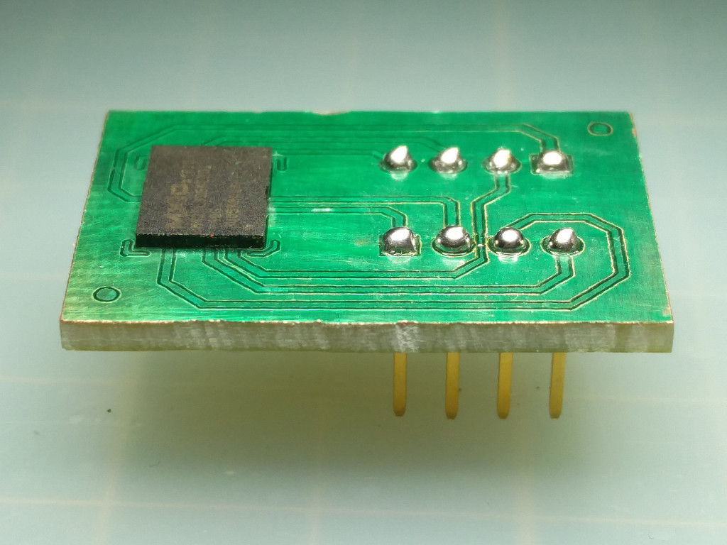
So all we need is a DIP8 socket and a nice breakout PCB.
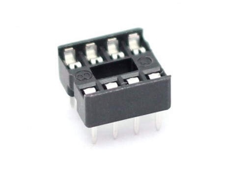
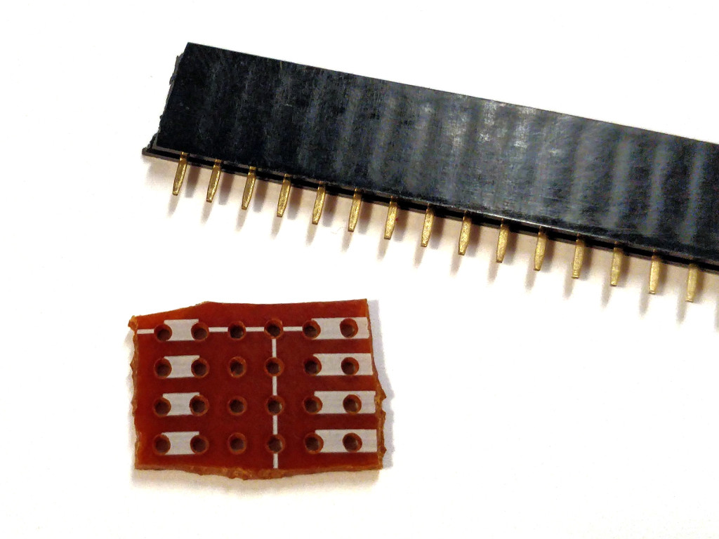
Or just whatever you happen to have in your drawers:
To connect the DIP8 female adapter to the IoT PCB, we need to do some microsoldering, i.e. soldering micro-wires wherever we can:
Either on a visible track, on the front or back layer;
Or on a via, if any;
Or at the end of the track, where it reaches a component;
Or simply on the BGA pads.
Soldering on tracks or end of tracks requires some reversing of the PCB routing and depending on the track width, this can be a delicate operation. See here an example of a 0.1 mm enamelled wire soldered on a 0.15 mm wide track, part of a challenge we designed for the Hardwear.io CTF.
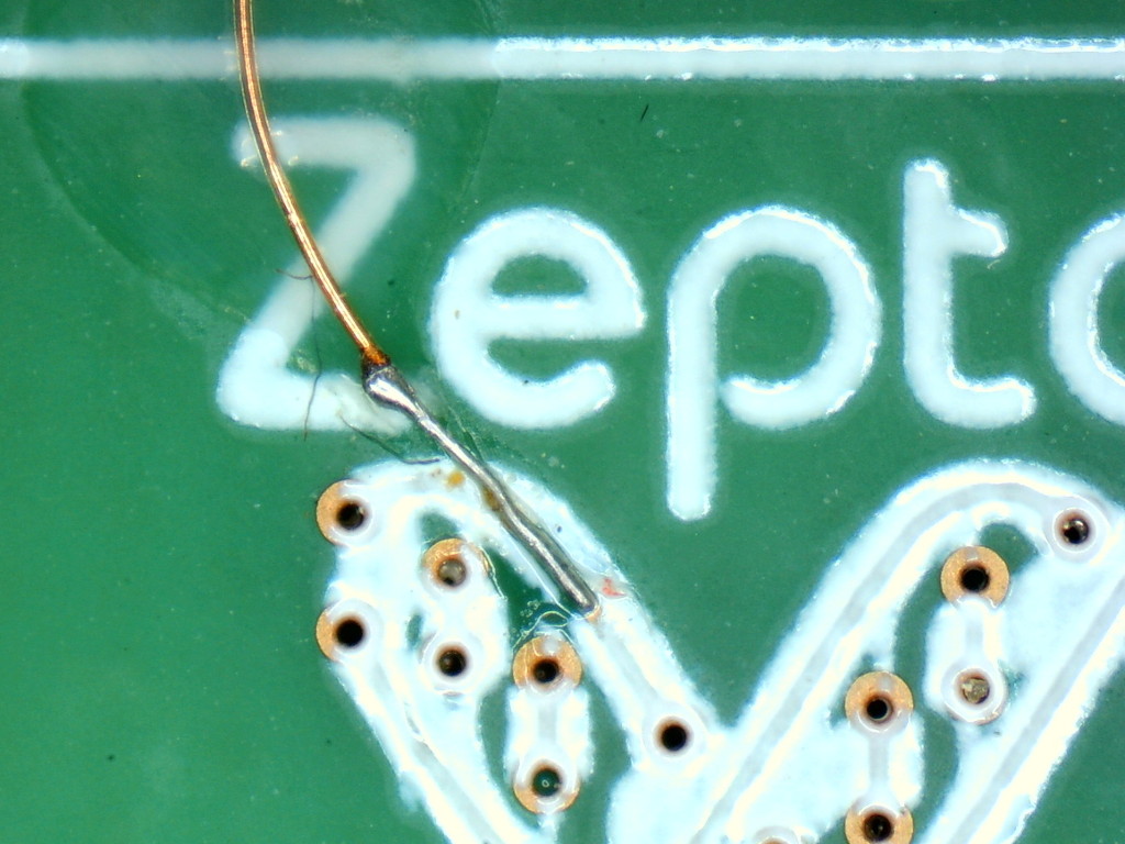
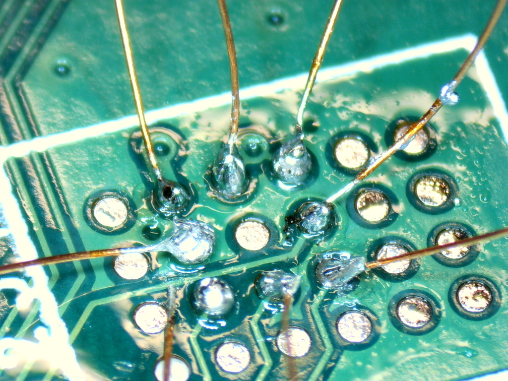
Back to our PCB, we decided to test some microsoldering directly on the BGA pads. They are readily available, we don't need to revert the routing, scratch any silk or mask and run everywhere to find a sweet spot. Still, a pad is much larger than a track and to control the amount of solder to bring to the spot, we reballed the pads we wanted to use.
Here is what it looks like. In this picture, there is still one wire to solder on the solder ball:
To reproduce this work, you can follow these steps:
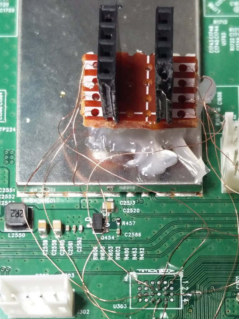
Solder the microwires on the DIP8 adapter, then secure it somewhere with some hot glue;
Remove with some desoldering wick the old solder on the BGA footprint on the PCB, that may be left from the previous heat-gun desoldering phase;
Clean residues with isopropanol;
Apply very little flux paste with a finger, just to get a sticky surface (too much would become liquid when heating later and balls would swim away);
Choose a proper ball size: about same size as the pad (which may be larger than the pad on the BGA side);
Position the solder balls with a microscope. No need to reball them all, just the 8 useful ones;
Beware the grid may be different from the one of the BGA, e.g. if the PCB can accommodate two different BGA footprints!;
Pre-heat the PCB so that its surface is about 150°C. This is not required when reballing a BGA but this is very important here! Some pads may be connected to large tracks or to ground areas and can't be reballed without proper preheating;
Apply gently some hot air with a heat gun to solder the balls on their pad. Take a large nozzle, it's easier (less blowing pressure, more even) and check with the microscope that balls don't fly away;
Wait for the balls to cool down; Melted balls are perfectly realigned, round and shiny, they tarnish and crumple when they cool down;
Prepare the microwires: use an iron with a large tip, put a large solder drop on its tip and you're ready to remove insulation and tin the tips of the microwires in one go: by sliding a tip under the solder dome. Wait about 3s. It should come back shiny and tinned. The solder on the iron becomes a messy blob after a minute or two, renew it from time to time by adding new solder;
Solder the microwires: check twice which wire goes where (and remember the grid may be different from the one of the BGA). Place a wire close to a pad with the tweezers, bend it if needed, then solder it with a very thin tip, using the solder of the balls. Some pads (e.g. grounded pad) may require a lot of heat. You may even have to use a larger tip for those ones to apply enough heat;
Secure the microwires: bend the microwires towards the PCB and secure them with a drop of UV glue.
If your hands shake, you can secure the microwires first with the UV glue, then bend them with the tweezers until they touch the solder balls. Then you just have to melt the solder.
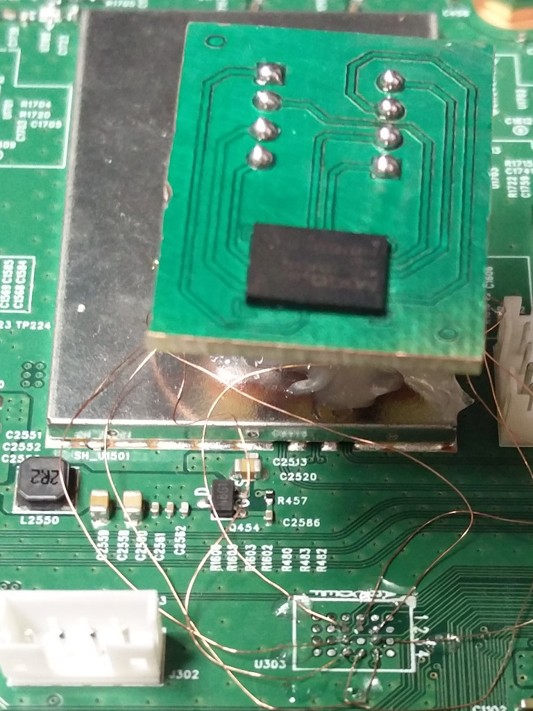
We're done, with the female DIP8 adapter in place:
The last thing to do is to plug back the flash chip into the device:
The device is working again :)
We're now in a very comfortable position to plug, unplug, read the memory content, mangle with it, reprogram it and test some hypotheses:
Can we swap the chip with the one of another device or are they bound to their MCU with some hardcoded chip ID?
Can we swap the content of the chip with the one of another device or is the memory content bound to some hardcoded chip ID?
Can we rollback snapshots?
Can we change parts of the memory image?
Are some parts protected by some CRC or some cryptographic signature?
etc.
Conclusion
That concludes our second article where we saw how to prepare the device to accommodate the flash chip with its adapter and how to start testing the security of the device.
Acknowledgements
Thanks to all Quarkslab colleagues who proofread this article and provided valuable feedback.