Authors Emma Benoit, Guillaume Heilles, Philippe Teuwen
Category Hardware
Tags PCB, flash, KiCAD, hardware, 2017
First part of a blog post series about our approach to dump a flash chip. In this article we describe how to desolder the flash, design and build the corresponding breakout board.
This blog post series will detail simple yet effective attacks against embedded devices non-volatile memories. This type of attack enables you to do the following:
read the content of a memory chip;
modify the content of a memory chip;
monitor the accesses from/to a memory chip and modifying them on the fly (Man-In-The-Middle attack).
In particular, the following topics will be discussed:
Desoldering of a flash chip;
Conception of a breakout board with KiCAD;
PCB fabrication and microsoldering;
Addition of a breakout board on an IoT device;
Dump of a SPI flash;
Dump of a parallel flash;
Man-in-the-Middle attacks.
Let's say you opened up yet-another-IoT-device and stumbled on a flash chip inside. Curious as you are, you obviously want to know what's going on inside.
Desoldering the flash chip
To read the content of the flash chip, there are basically two options :
connecting wires directly on the pins of the chip;
desoldering the flash and plug it on another board.
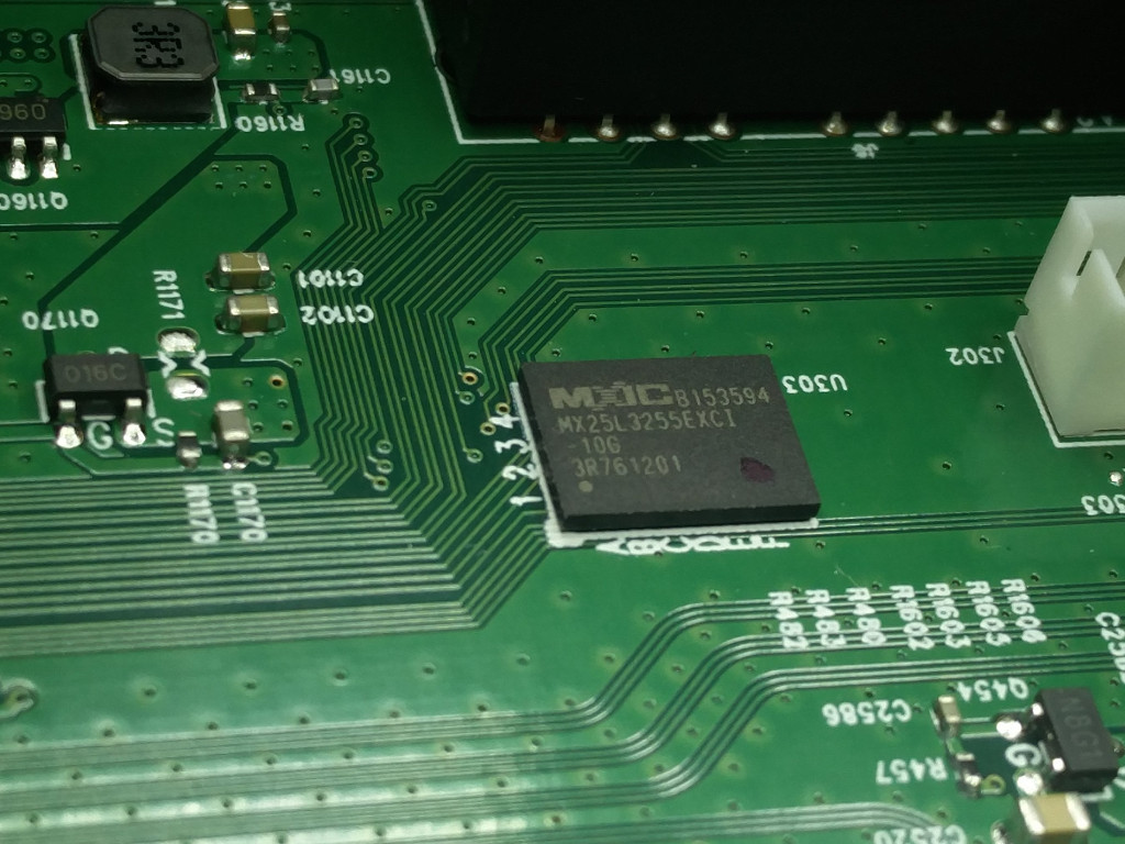
One of the things to consider when choosing a method to read the chip is the packaging of the integrated circuit (IC). For example, connecting wires directly on the pins of the chip works well with chips using a quad flat pack (QFP) packaging, but it's less adapted if there are no visible pins. In the following case, the flash chip uses a ball grid array (BGA) packaging, which means no visible pin to fiddle with, so we choose to desolder the IC.
Picture of our target chip:
On the bright side:
Since we're extracting the flash, all possible interferences with the onboard microcontroller are avoided.
The chip is removed completely from the board, which gives us the ability to study the PCB underneath and find out the routing to the flash chip.
The original chip can be replaced with something else (another chip, a microcontroller, ...).
On the less bright side:
The board cannot run without all of its components, you'll have to solder it back if you want to use it in the future.
Some nearby components could be damaged during the extraction.
The flash chip itself could be damaged if it's done improperly.
So... desoldering flash, right? If you never tried desoldering electronic components before, the tricky part is to melt the solder on all pins at the same time. There are several techniques to do that. We choose to go with the heat gun. The goal is to heat the area where the chip is, wait for the solder to melt and remove the chip.
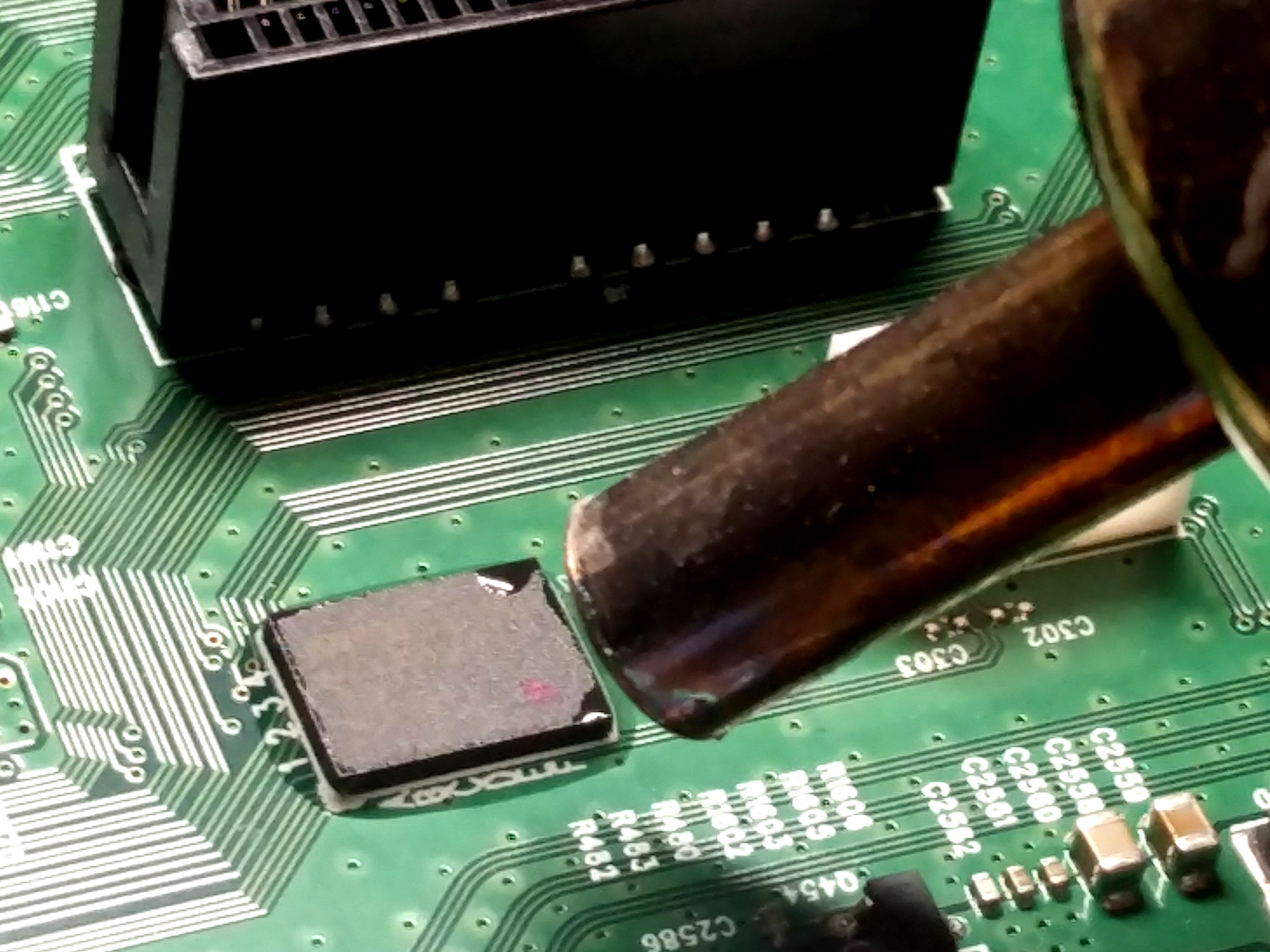
This technique is simple and rapid but it tends to desolder adjacent components, so be careful not to move them (i.e. this is exactly the worst moment to sneeze).
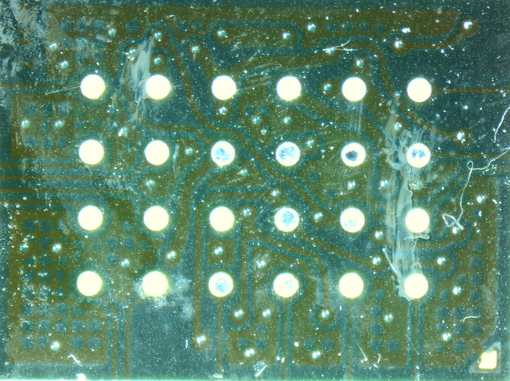
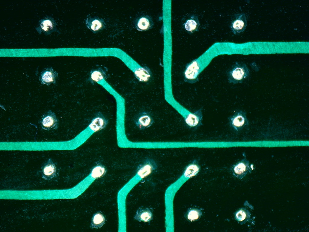
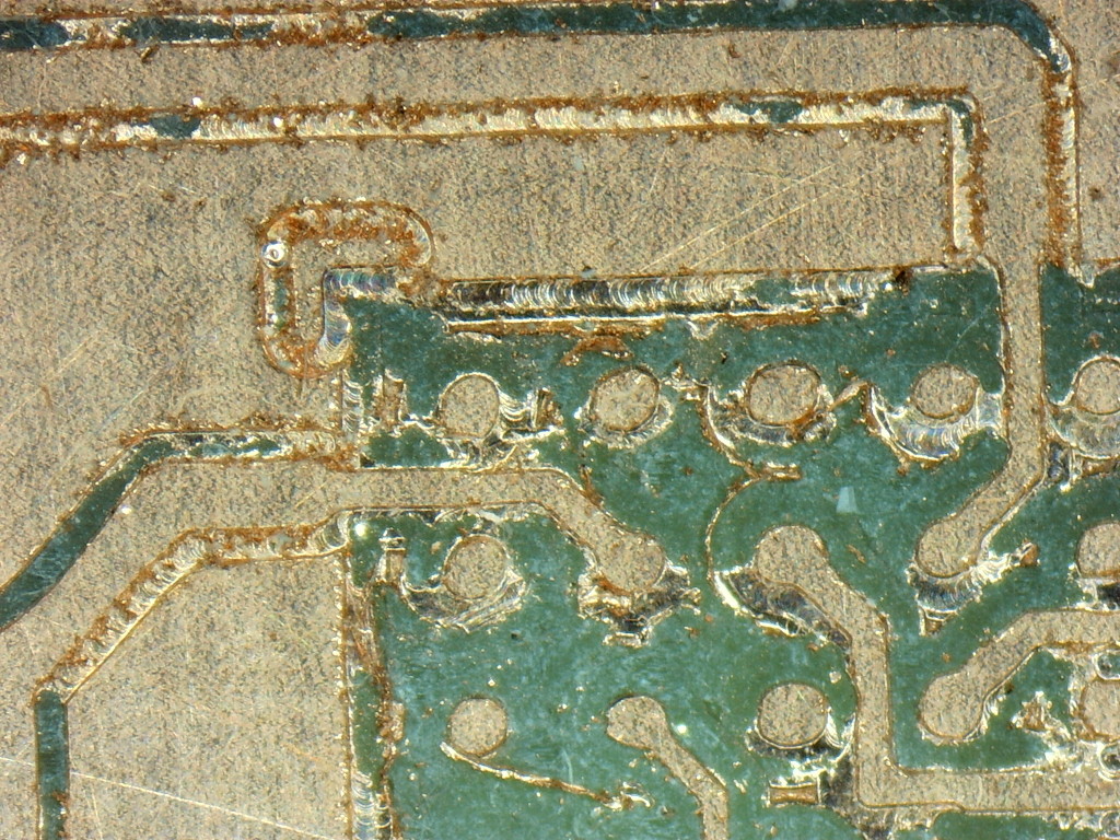
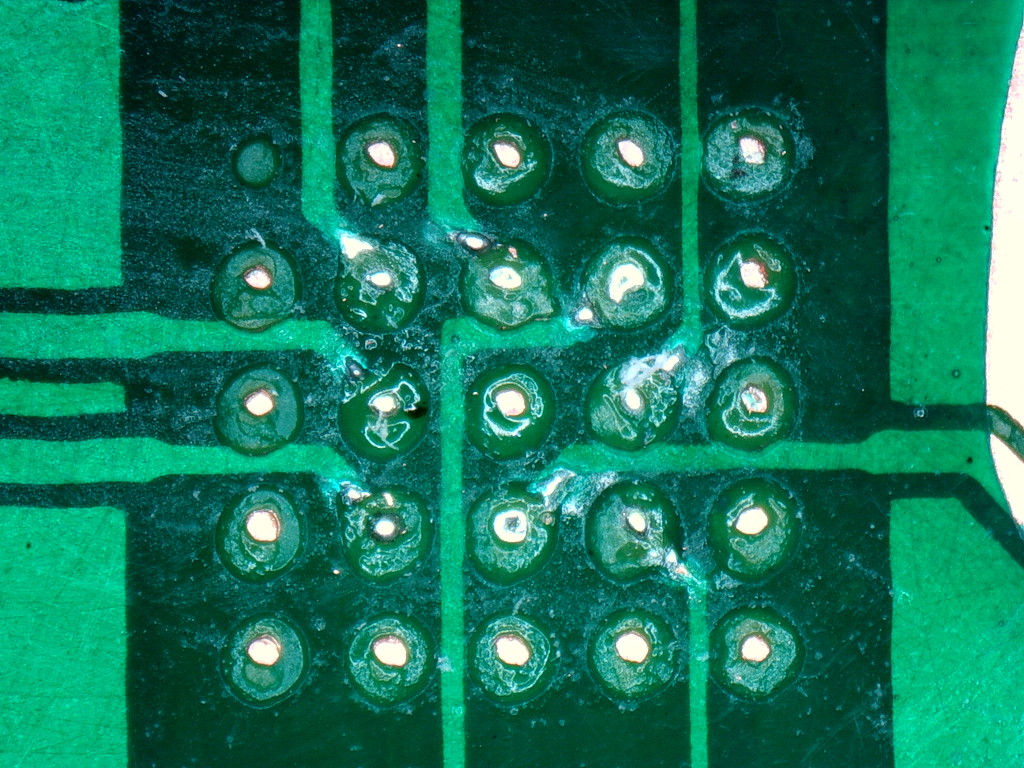
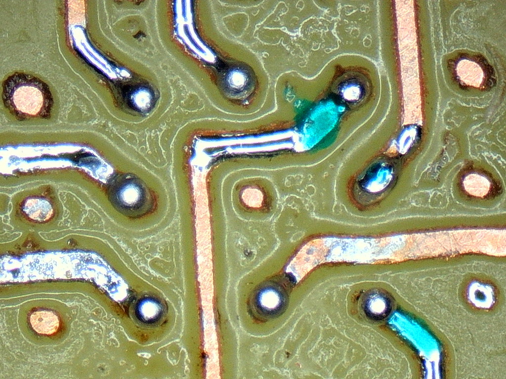
The picture below shows our chip out of its emplacement and we can now have a look at the PCB routing. We can already make some hypothesis, like the two bottom rows which are likely unused since they are not routed.
Conception of a breakout board with KiCAD
What do we do now with that chip? BGA layouts are a mess, you can have a 5x5 grid or a 4x6 grid for the exact same chip. Pinouts are equally fun, and usually specific to the chip. Another thing you might be wondering is how to access a particular pin when they are all packed together in a grid like that?
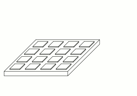
One solution is to make a breakout board! Basically, a breakout board mirrors all the pins of the chip but with more space between them, so you can access them easily.
To realize this, we first need to gather some information about the chip itself. Most of the time, the brand and/or model are written on the chip and help identifying it. With this information, one can look for the corresponding datasheets. If you can't identify the chip or if you can't find the datasheet, you will have to do some reverse engineering on the PCB to identify each signal.
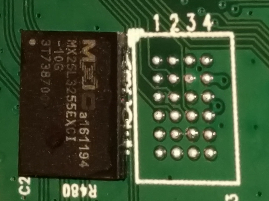
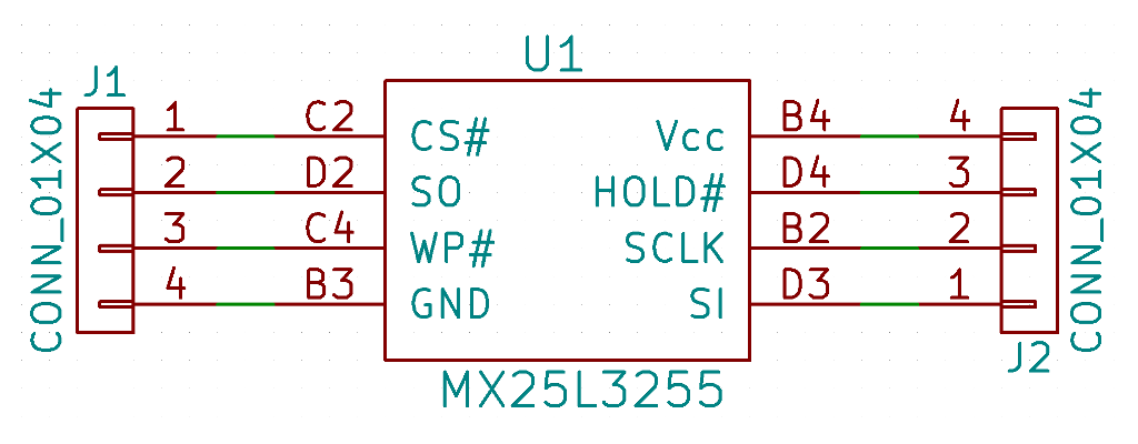
The brand is indicated on the first line of our chip: MXIC stands for Macronix International. The second line is the model of the chip, which leads us to the MX25L3255EXCI datasheet.
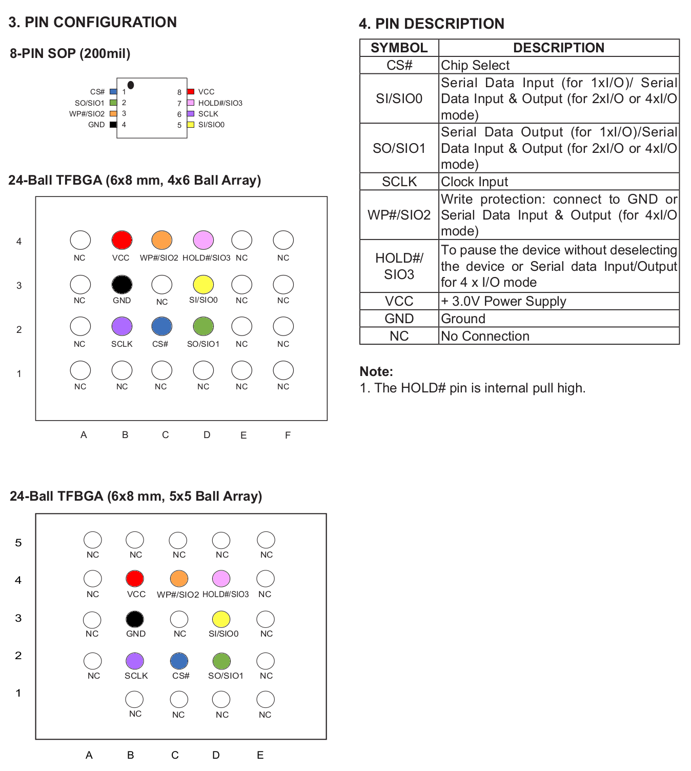
The section that is of interest to us is the pin layout, page 7 of the datasheet. Both BGA configurations (4x6 and 5x5) are described as well as a SOP8 package. We can see that only eight pins are useful, other pins are tagged "NC" which means "no connection".
To communicate with the flash chip, we need a PCB exporting all the required pins to some easy-to-access header.
The design of the PCB can be realized using KiCAD, one of the most popular electronics design automation (EDA) software.
If you are not familiar with KiCAD, many great tutorials are available like KiCAD Quick-Start Tutorial.
The design of a breakout board follows the same process as for any other board:
Create an electronic schematic for your board in eeschema, and define the components that are specific to your project, for example your flash chip.
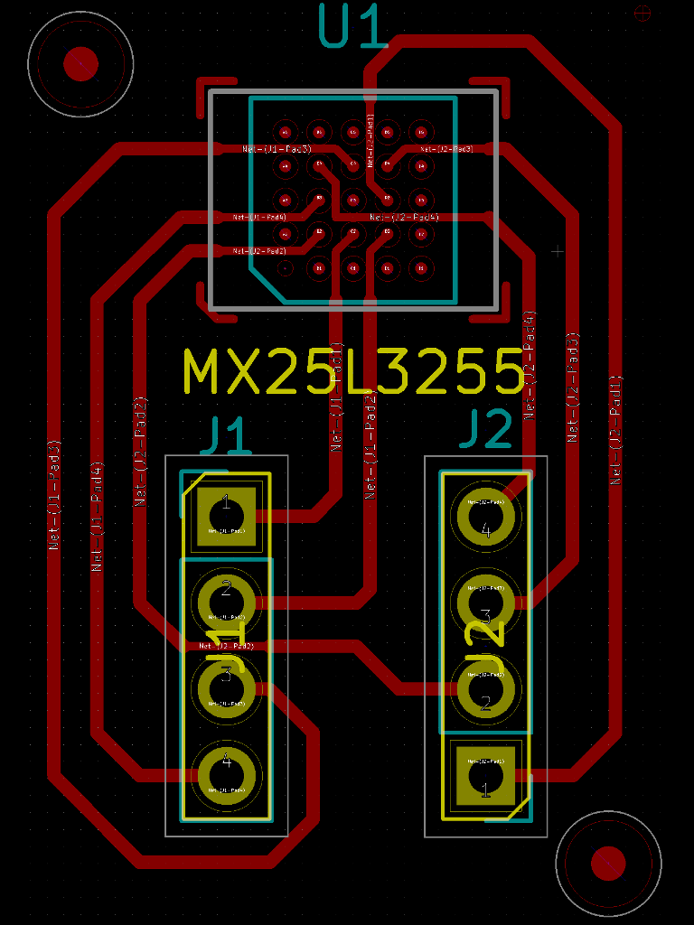
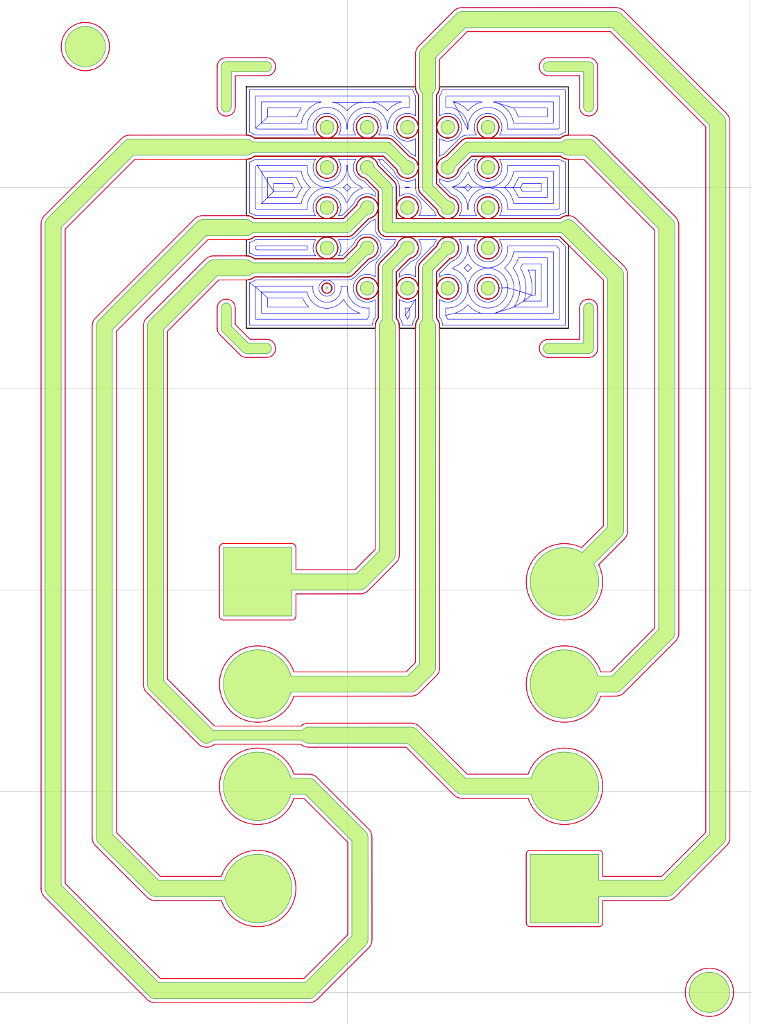
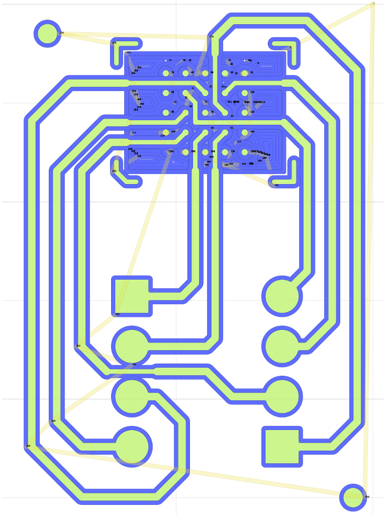
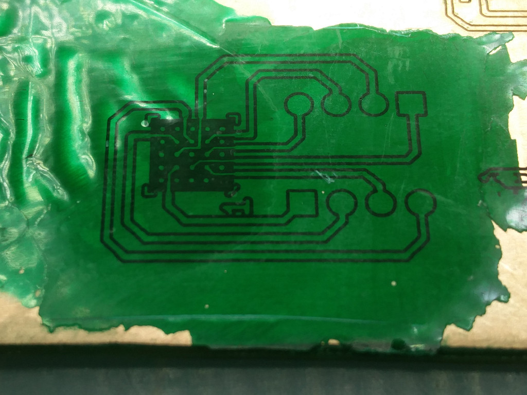
Create the specific footprint for your flash chip in pcbnew. This is where the information from the datasheet that we looked earlier is useful. We will add a 4x6 grid representing the BGA grid, and two 1x4 connectors linked to the 8 useful pins. The final step is to add routes to connect our components
Our design is done, how do we transform a KiCAD project into a working PCB?
PCB fabrication
A PCB is basically a sandwich made of a layer of substrate between two layers of copper. The substrate is usually made of FR-4 (glass-reinforced epoxy laminate) but other cheaper materials can also be found. Routes are traced on the copper layer and the excess copper is then removed.
Several techniques exist to remove the unwanted copper, we tried the following:
Etching;
CNC milling.
Both techniques are detailed, as we used the etching technique to build the 4x6 BGA PCB and the milling technique was used to build the 5x5 BGA PCB.
Etching
Etching refers to the process of using a chemical component to "bite" into the unprotected surface of a metal. We use ink as a way to delimit the traces and protect the bits of copper to keep.
We use the toner transfer method to reproduce the design on copper. The design is printed on a glossy sheet of paper using a laser printer. The sheet of paper is then taped to the piece of copper/fiber glass substrate, and heat and pressure are applied to get the design out of the paper onto the copper board. Usually, this technique uses a regular clothes iron to apply heat and pressure. We found out that using a laminator is way more efficient as the heat and the pressure applied are more uniform.
Next step is the actual etching. The board is immersed into a chemical solution which will remove excess copper, except where the toner is.
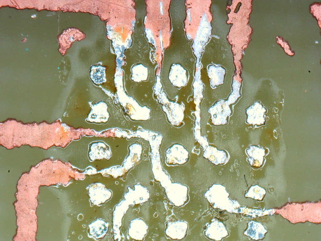
Our breakout board after etching, still with the transferred toner attached:
And after removing the toner with acetone:
The PCB board is now ready for microsoldering. Microsoldering is like soldering but with tiny components, hence it requires a microscope.
Another difference with traditional soldering is the packaging of the solder. Traditional soldering uses solder in the form of wire while BGA microsoldering uses solder balls.
Next, we can start reballing:
put a new solder ball in each slot and apply heat to melt the solder balls in place;
align the chip and the board;
reflow.
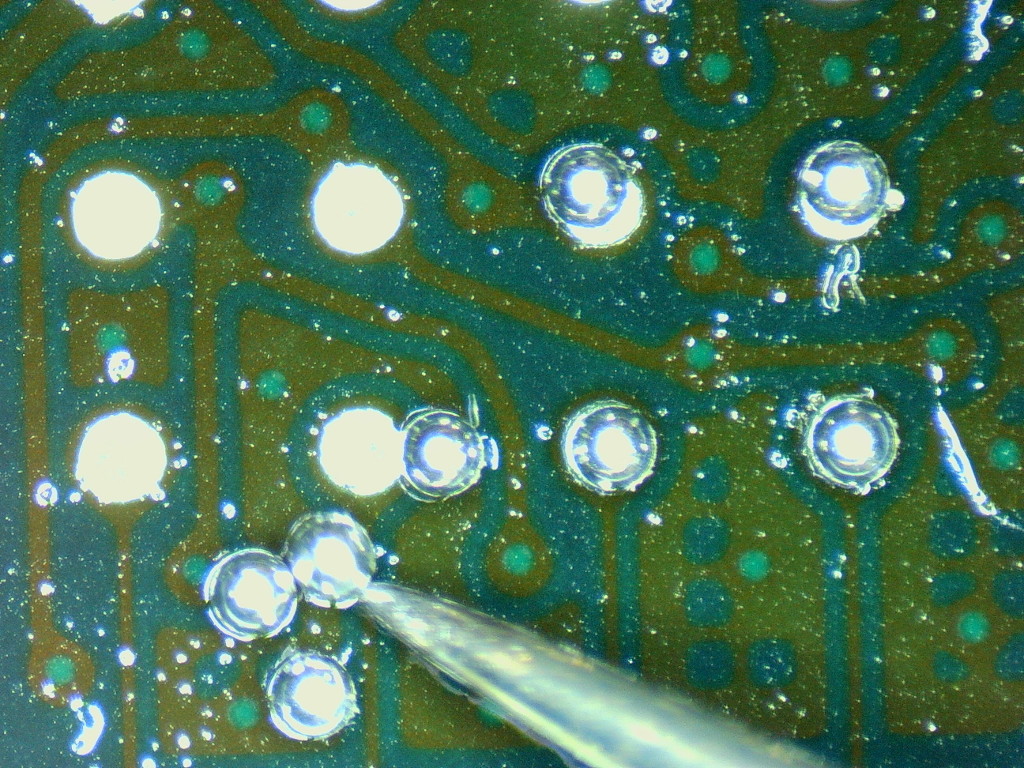
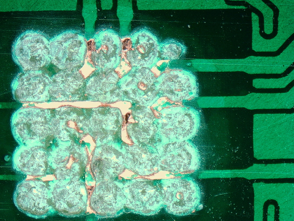
The board being reballed:
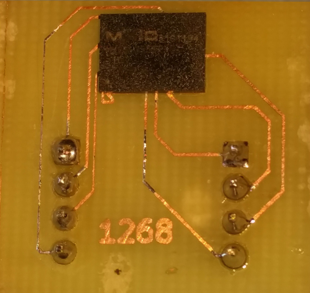
And the final result with the chip and the board after microsoldering:
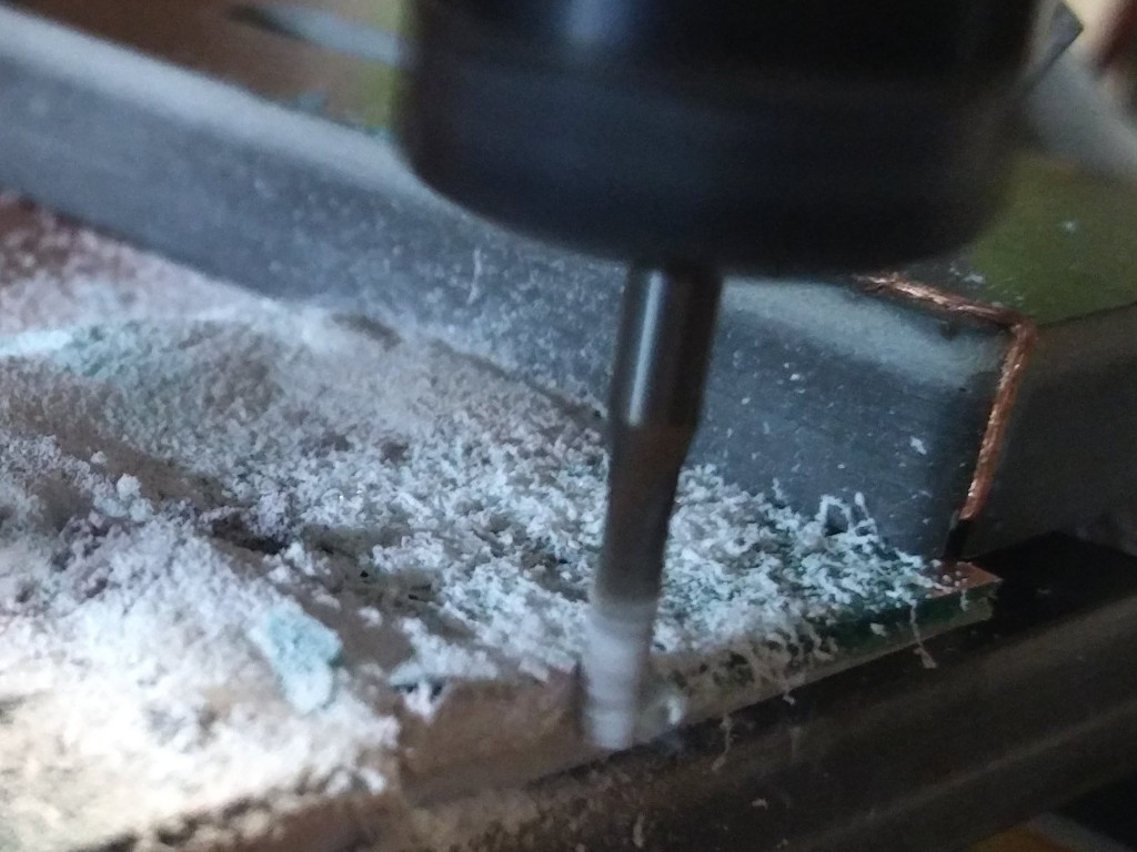
CNC Milling
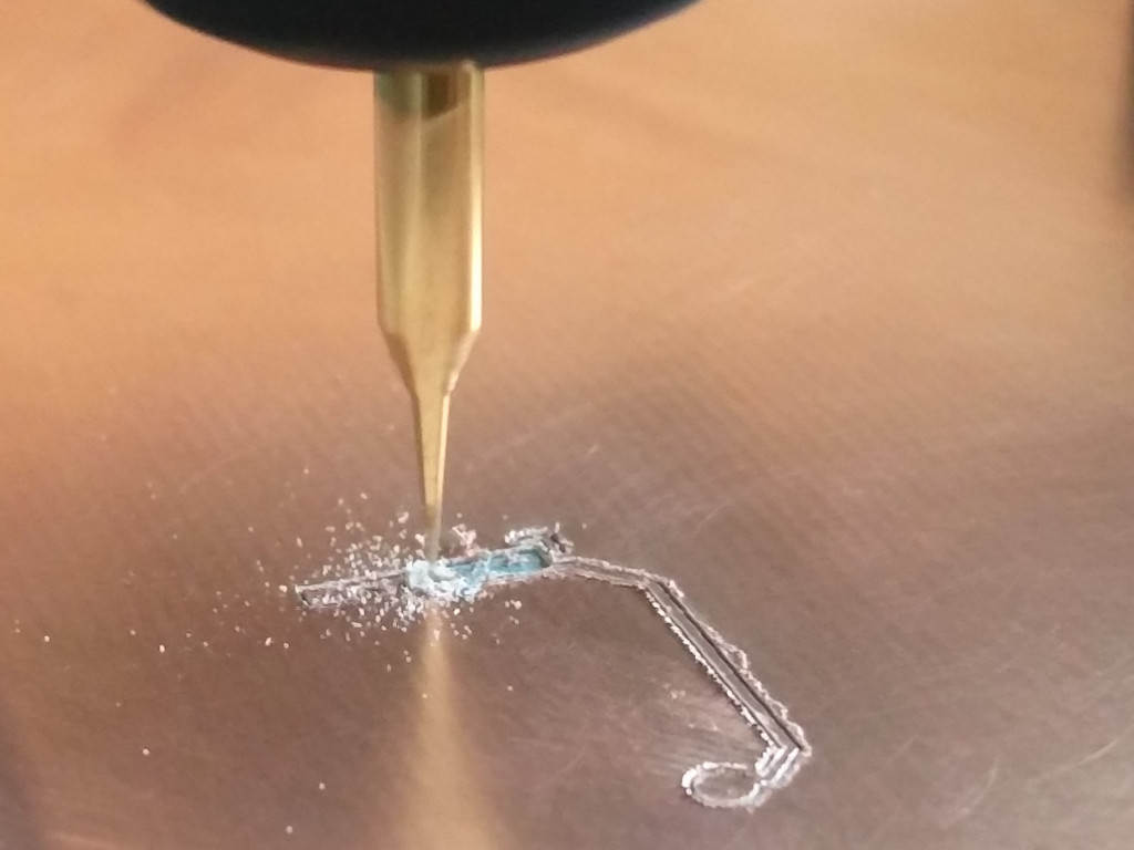
Alternatively, a CNC milling machine can be used to carve out bits of unwanted copper. Actually rather than removing all the unwanted copper, the CNC will simply isolate the required tracks and leave the excess of copper in place.
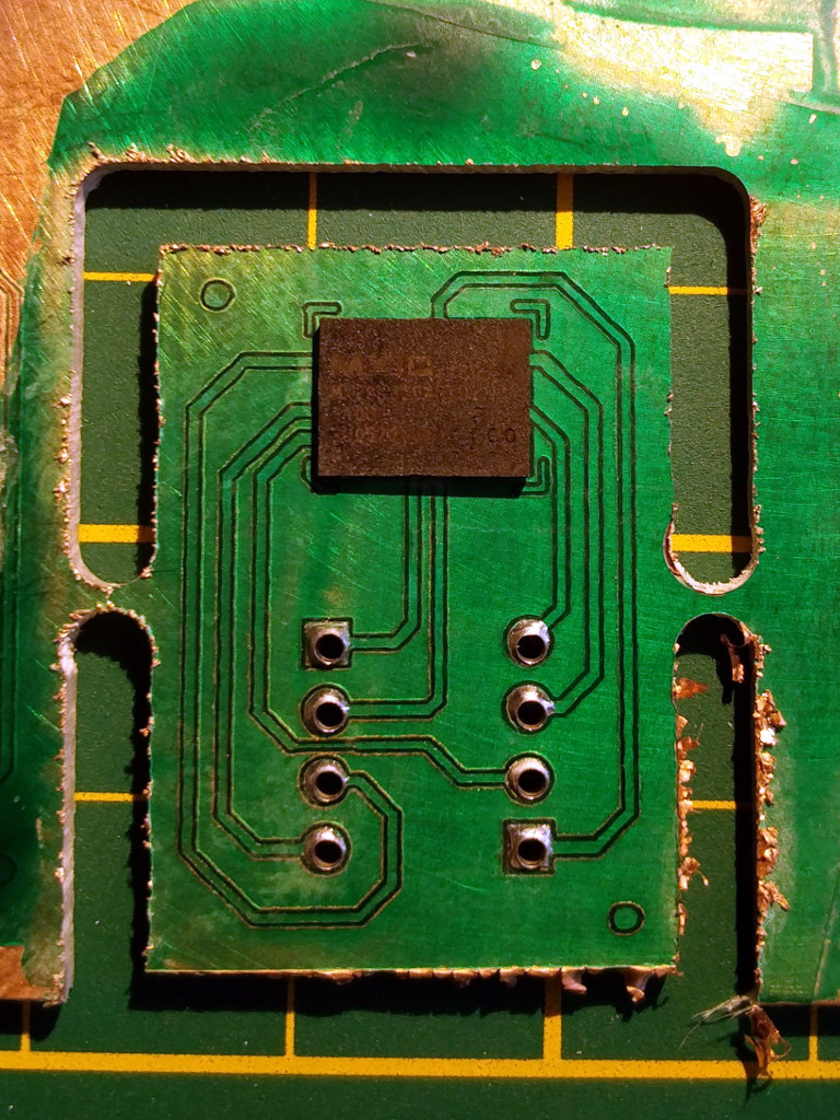
1. The 5x5 BGA format was used to build a PCB. While the 4x6 version was a breakout board, we designed the 5x5 version such that it can be directly plugged in a universal EEPROM programmer ZIF socket. As we've seen in the datasheet, this chip also exists in SOP8 package, so we've chosen to mimic a DIP8 pin header reproducing the same pin layout as for the SOP8. So for the universal EEPROM programmer, this setup will be virtually the same as reading the SOP8 chip via a classic SOP8-DIP8 adapter.
2. The footprint for the chip is somehow similar to the one we designed for the 4x6 but with a 5x5 grid, the 1x4 connectors closer, as for a DIP8, and a somehow more tortuous routing to respect the SOP8 layout which is unfortunately completely different from the BGA one.
3. KiCAD is not able to produce directly a file compatible with a CNC, therefore we'll use Flatcam which takes a Gerber file and allows to define a path for the CNC to isolate the desired copper tracks. To avoid shortage issues, we also define an area under the BGA chip to remove entirely the unwanted copper.
4. And we pass the produced STL file to bCNC, in charge of controlling the CNC. It has some nice features such as auto-levelling, i.e. measuring the actual height of the board in several points (because nothing is perfectly flat), and producing the heat map you can see in the snapshot below.
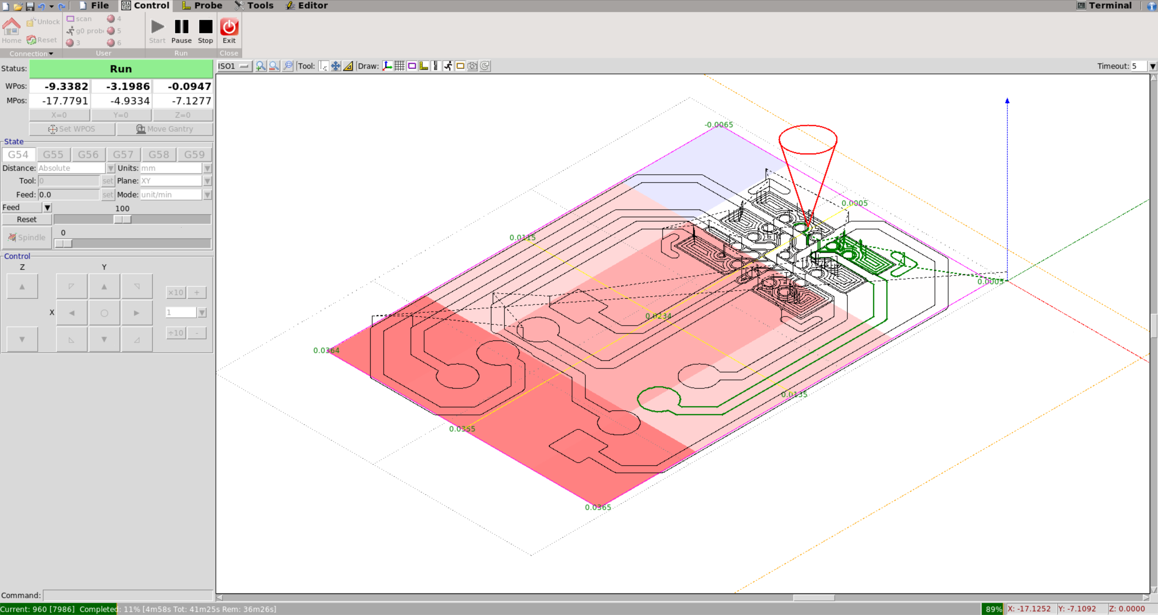
Milling in action, corresponding to the tracks highlighted in green in bCNC:
Board fully milled:
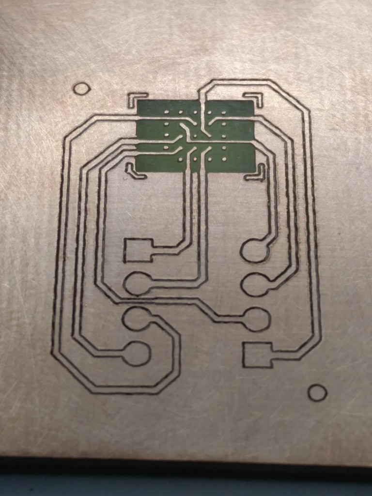
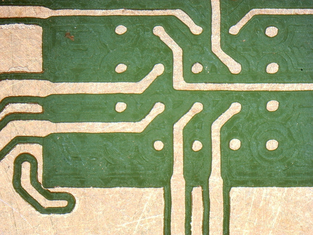
Close up of the final result where we can distinguish the pattern of the flatcam geometry path under the BGA:
6. Next, we apply some solder mask, which is the characteristic green layer protecting the copper from oxidation, and cure it with UV light.
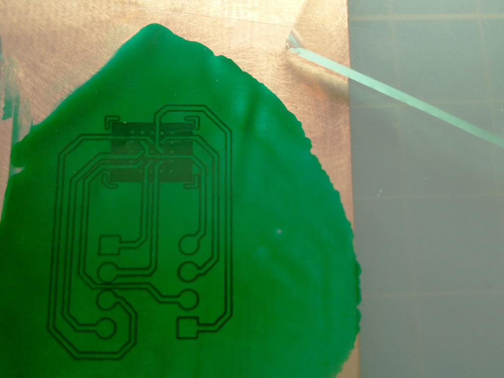
7. The solder mask covered the pads of the BGA and of the 1x4 connectors, they are unusable like this. We scratch manually the thin layer of paint to free the pads.
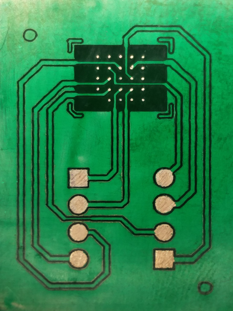
Tinning step, where we apply solder on all pads:
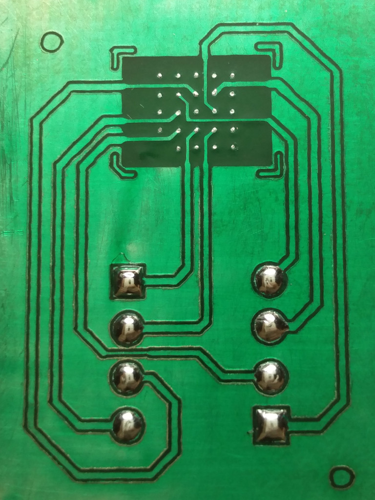
Back to the CNC to drill the holes and cut the edges of the board:
Final board with the BGA chip soldered and ready to be inserted in a universal EEPROM programmer:
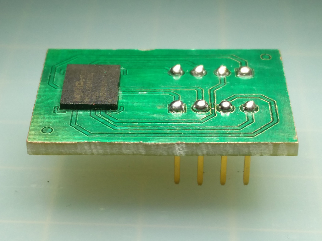
As we've chosen to mimic the SOP8 pinout, we've simply to tell to the programmer that our chip is the SOP8 version!
Bonus: the horror show
Here is a compilation of our best failures, because things don't always go as planned, but we learned a lot through these experimentations and we are now ready for the next IoT stuff :)
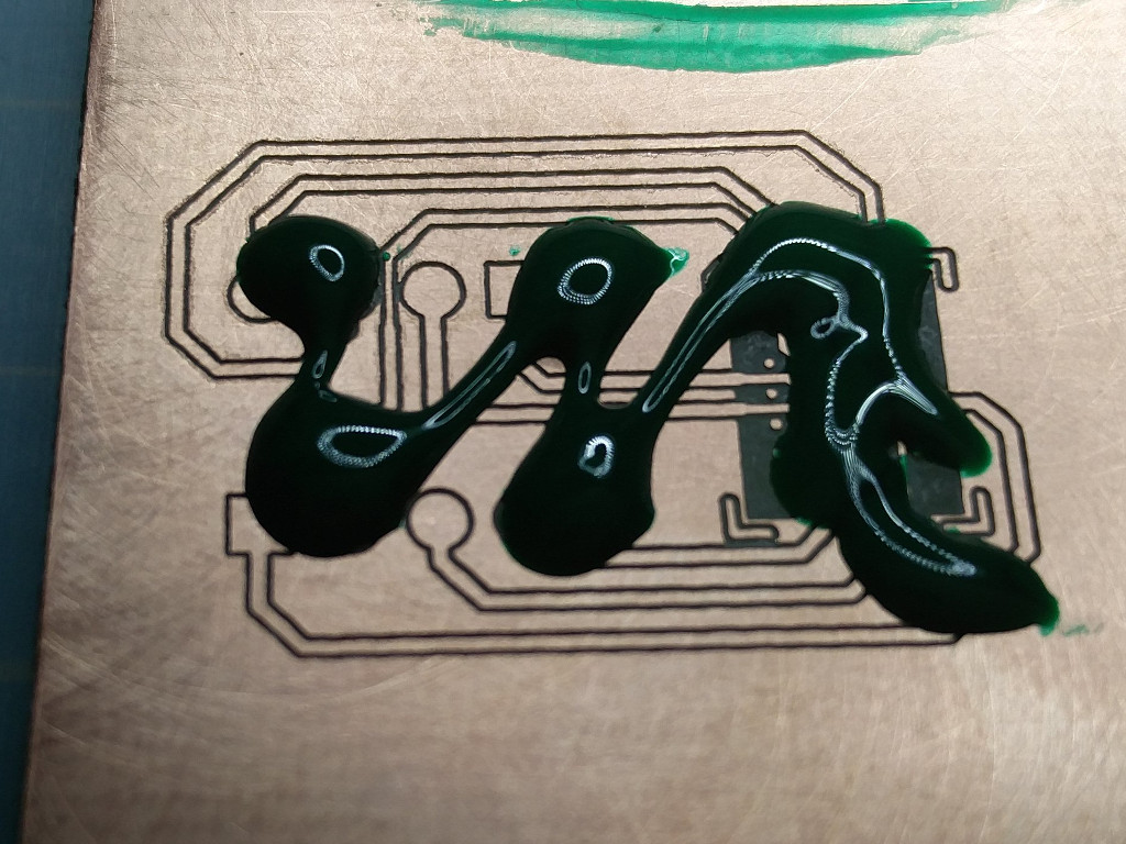
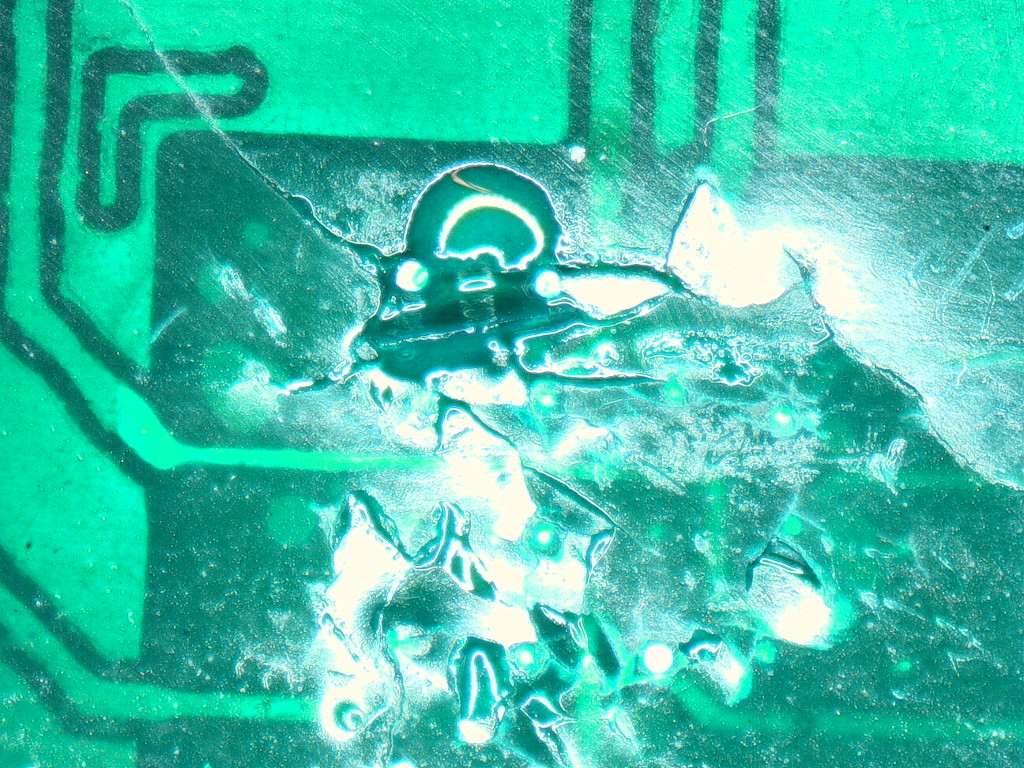
Toner transfer is not always as easy as it sounds...
Milling on the CNC with the right depth neither...
Failing at finding a plastic that doesn't adhere to the green mask... (eventually IKEA freezing bags revealed to work very well :) )
Attempt to mill the green mask...
Second attempt with a tool mounted on a spring: looks almost good but actually all tracks were cut from the pads...
Third attempt by adding first some solder in the hope to make them thicker
Created a lake of green mask too thick to cure with UV light, and when the surface of the icy lake breaks...
Conclusion
That concludes our first article where we saw how to desolder a flash, design a PCB and detailed two techniques of PCB fabrication.
Acknowledgements
Thanks to all Quarkslab colleagues who proofread this article and provided valuable feedback.