Author Elouan Appere
Category Reverse-Engineering
Tags secure boot, reverse-engineering, Qualcomm, exploitation, 2019
Qualcomm is the market-dominant hardware vendor for non-Apple smartphones. Considering the [SoCs] they produce are predominant, it has become increasingly interesting to reverse-engineer and take over their boot chain in order to get a hold onto the highest-privileged components while they are executing. Ultimately, the objective is to be able to experiment with closed-source and/or undocumented components such as hardware registers or Trusted Execution Environment Software.
Introduction
From March to September 2019, I had the pleasure to do a six-month internship at Quarkslab to study the boot chains produced by Qualcomm and complete the following tasks:
get the highest privilege level (EL3) to execute code;
dump high-level privilege components such as the bootROM or Primary Boot Loader (PBL), the Secondary Boot Loader (SBL) and reverse-engineer them;
take over the boot chain;
study Qualcomm's Secure Monitor and undocumented secure registers such as the "XPU" registers.
Two different phone models were used to perform this research: a Google Nexus 6P and a Nokia 6.
Given how widespread Qualcomm hardware is, as stated above, many people have already worked on studying Qualcomm components. In particular, Aleph Security released a series of 5 blogposts (aleph aleph2 aleph3 aleph4 aleph5) (alongside tools), describing how they took over the Nokia 6 boot chain and wrote a debugger. These blogposts served as basis for our own work.
First of all a general overview of the Secure Boot process and especially the one used by Qualcomm is given, then by using Aleph Security's tools, we will dump the Nexus 6P and Nokia 6 bootroms in order to gain code execution in them and inject a small debugger, giving the ability to dump the whole phone from the very beginning. This section will also explain the difficulties we encountered with the payload provided by Aleph Security, and how we managed to get around them. After propagating the control to the next stages of the bootchain, we patched the Qualcomm Secure Execution Environment to add a hook giving us a read/write primitive in the highest privileg level EL3. Finally, we will discuss briefly about the XPU register.
Context
Armv8 Exception Levels
Armv8 systems have multiple privilege levels, called exception levels or ELs, ranging from EL0 to EL3. The lower the exception level number is, the less privileges it has. Additionally, with the software and hardware isolation provided by the TrustZone technology, Armv8 distinguishes between the Non-Secure and Secure exception levels.
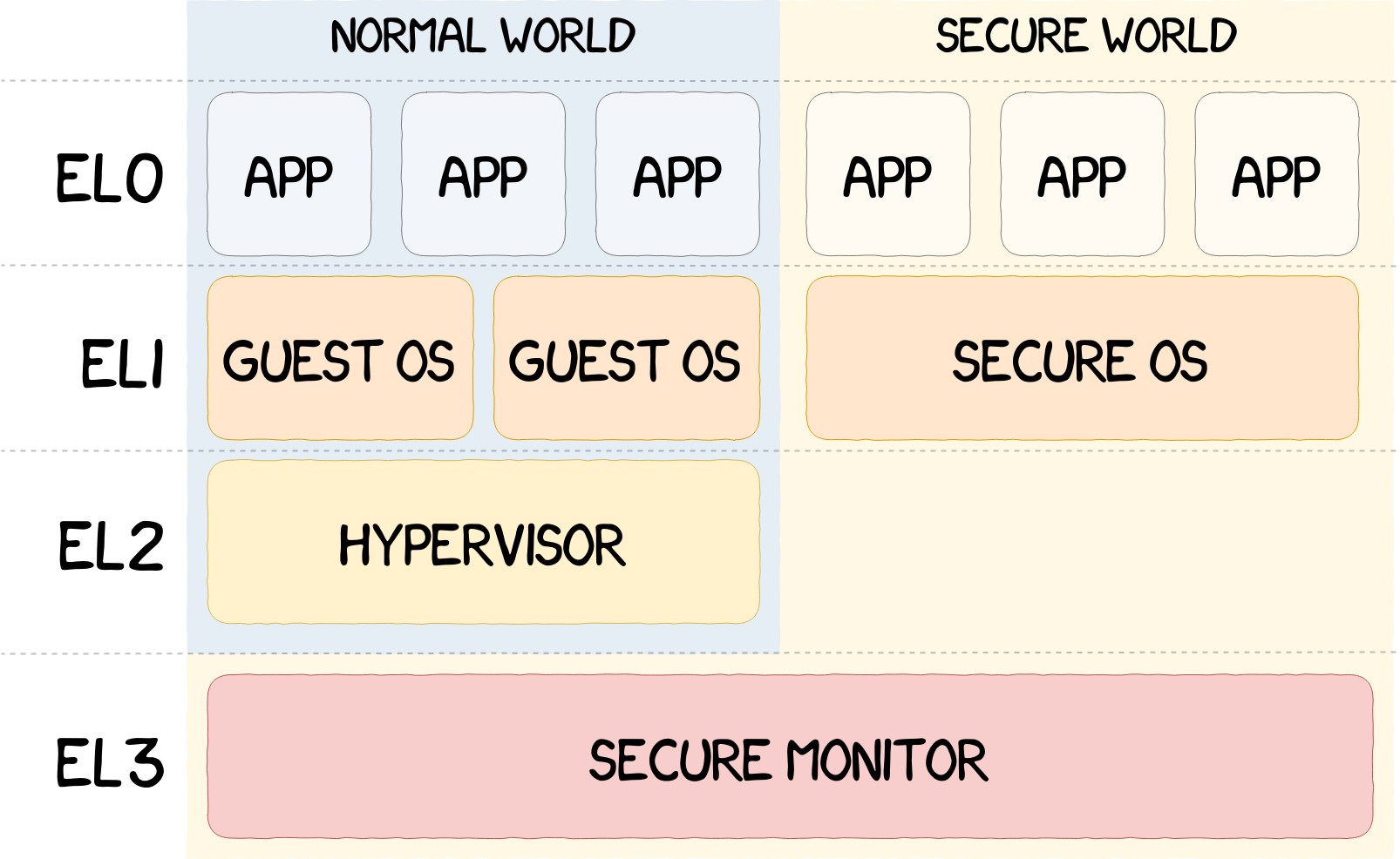
Armv8.4 and later revisions add the previously missing Secure EL2 exception level.
Secure Boot
General Overview
A secure boot chain is a chain where every stage loads, authenticates (with e.g. RSA) and then executes the next one. The very first stage, the bootROM, is implicitely trusted, as it is most often stored on a CPU die. While modifying it may be considered feasible in theory, it is not scalable. The result is a full chain of trusted components:
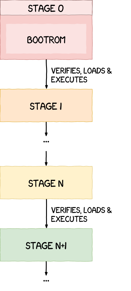
According to Qualcomm Secure Boot and Image Authentication Technical Overview document [QualcommSB], the binary authentication is designed more or less in the following way:
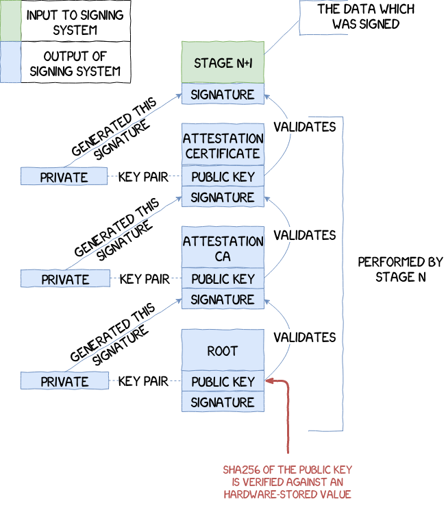
The vendor emits a root certificate, keeping the private key for themselves and using the public key in the bootROM. As it has to be implicitely trusted, a hash of its public key is stored in hardware (most of the time, in fuses), to ensure it has not been tampered with.
This certificate can sign another certificate (and so on...), or directly authenticate a signature. The end result is a certificate chain where different parties can sign various sub-components of the system.
Qualcomm's Secure Boot chain
Design
The Qualcomm secure boot chain, on non-Samsung devices, is designed as follows:
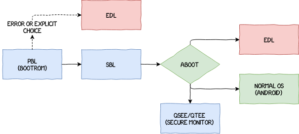
the bootROM, also called PBL (Primary Boot Loader), is the first component to be executed by the CPU;
the next component, the SBL (Secondary Boot Loader), used to be divided in SBL1, SBL2 and SBL3 in older hardware revisions:
this is now the XBL (eXtended Boot Loader);
the SBL loads the Secure Monitor, QSEE (now QTEE), and executes it in EL3. It also loads aboot (now ABL, both standing for Android Boot Loader) and has it executed in EL1;
aboot (or ABL) loads either the regular OS, or a recovery version of it; it can also communicate with a PC via USB using the fastboot protocol.
EDL
More importantly, the PBL (bootROM) can execute a recovery mode, called Emergency Download Mode (EDL), if one of the following conditions is met:
the SBL is corrupt and/or its version is invalid;
specific testpoints have been shortened on the board;
the system reboots and specifies that the bootROM needs to transition to EDL mode (implementation details vary from one SoC to another).
When going to EDL, the bootROM waits for the PC to send commands. Among these commands, a particularly interesting one is used to send a signed image over USB. To alleviate this task, Aleph Security created a tool named firehorse.
On older telephone models, EDL images ("programmers") have interesting properties, among which are:
some signed images are available on the internet depending on the phone model;
programmers execute in EL3;
they have arbitrary read and write commands (peek and poke).
Exploiting the Nexus 6P
The Google Nexus6P, codenamed angler, is a phone co-developed by Google and Huawei released in late 2015. Its SoC is a MSM8994.
Accessing EDL Mode
Accessing EDL mode is fairly trivial on this phone. It is sufficient to downgrade the phone to a version older than December 2017 — which is trivial because Google themselves give you the needed images and instructions [OTA] — and root it. Once rooted, one simply needs to execute the following commands to access the EDL mode:
echo 1 > /sys/module/msm_poweroff/parameters/enable_edl
adb reboot edl
Dumping the BootROM (PBL)
Once the device has entered EDL mode, it identifies itself as Qualcomm HS-USB 9008 and the bootROM waits for commands.
It is then necessary for the PC to communicate with the phone to send the signed EDL image. Using Aleph's tool, firehorse, which is a wrapper for Qualcomm's official tools, the command is:
firehorse -c COM3 -t angler fw hello
Assuming the phone is mapped to COM3, and that the EDL image (or programmer) is at its correct location.
Knowing the address of the bootROM thanks to Aleph blogposts, it is trivial to dump the bootROM (PBL):
firehorse -c COM3 -t angler fw peek 0xFC010000 0x20000 pbl.bin
In any case, the bootROM is mirrored at physical address 0 too.
Gaining Code Execution
Once we can communicate with the EDL programmer, it is possible to use the poke command to write at any address as explained in the Aleph's third blogpost aleph3. With the powerfull primitive, it's possible to inject code directly on the stack.
However, on Aarch64 EDL programmers, SCTLR_EL3.WXN is a protection mitigating such attempts.
One way this can be worked around is by using ROP (return-oriented programming), which is what Aleph tried to do. However, their ROP chain did not seem to work during our tests and we decided to try a different approach by modifying page table entries. By mapping the 1GB region containing our code as read-only, we can subsequently make our code executable. Moreover, since the virtual address range is otherwise unused, no TLB (Translation lookaside buffer) flush is required. Using the firehorse code base, this gives:
addr = 0xFC100000
path = r"hooks.bin"
target = t.get()
ttbr0 = target.page_table_base
FH_FW.upload64(addr, path)
I("uploaded payload")

FH_FW.poke64(ttbr0, 0xC0000611) # AP=0b10, read only; map 1GB from 0xC0000000 to VA 0
FH_FW.poke64(target.saved_lr_addr, addr + 4 - 0xC0000000) # jump to our code at addr
We've tried disabling SCTLR_EL3.WXN as soon as we gained code execution. Unfortunately, this did not work; we thus had to disable the MMU with the following gadget:
.text:00000000F803DF38             loc_F803DF38                            ; CODE XREF: write_sctlr+C↑j
.text:00000000F803DF38 01 10 1E D5                 MSR             SCTLR_EL3, X1
.text:00000000F803DF3C
.text:00000000F803DF3C             locret_F803DF3C                         ; CODE XREF: write_sctlr+14↑j
.text:00000000F803DF3C C0 03 5F D6                 RET
With this done, we can now try to take over the Nexus 6P boot chain.
Taking Over the Bootchain: First Attempts
Given that, on the Google Nexus 6P, the bootROM is executing Aarch32 code (i.e. 32-bit) while the EDL is a 64-bit image, it immediately comes to mind that we need to reset the CPU back into Aarch32 mode.
We thus tried to write the reset address to the same hardware register that is used by the bootROM to set the 64-bit entry address, 0xF900D07C, then use the standard Armv8 register, RMR_EL3, to actually reset the CPU.
However, after a few tests, it turned out that this doesn't work:
the bootROM is mirrored at the physical address 0; this probably means that the Aarch32 reset vector is hardcoded at address 0;
just resetting the CPU without trying to change the entry address doesn't work either; this may indicate some weird hardware issue.
Reversing the Nexus 6P BootROM
The execution of the bootROM, also called PBL, starts at address 0xFC010000, which directly jumps to 0xFC010050, then 0xFC010054. This corresponds to the following code:
RAM:FC010754 50 0F 0D EE                 MCR             TPIDRURW, R0
RAM:FC010758 90 1F 0D EE                 MCR             TPIDRPRW, R1
RAM:FC01075C B0 0F 10 EE                 MRC             R0, MPIDR
RAM:FC010760 0F 00 00 E2                 AND             R0, R0, #0xF
RAM:FC010764 00 00 50 E3                 CMP             R0, #0
RAM:FC010768 5B 00 00 1A                 BNE             loc_FC0108DC
RAM:FC01076C 48 03 9F E5                 LDR             R0, =0xFC010000
RAM:FC010770 10 0F 0C EE                 MCR             VBAR, R0
RAM:FC010774 44 13 9F E5                 LDR             R1, =0xFC400204
RAM:FC010778 00 00 91 E5                 LDR             R0, [R1]
RAM:FC01077C 01 00 80 E3                 ORR             R0, R0, #1
RAM:FC010780 00 00 81 E5                 STR             R0, [R1]
RAM:FC010784 38 13 9F E5                 LDR             R1, =0xFC400208
RAM:FC010788 00 00 91 E5                 LDR             R0, [R1]
RAM:FC01078C 01 00 80 E3                 ORR             R0, R0, #1
RAM:FC010790 00 00 81 E5                 STR             R0, [R1]
The bootROM starts by setting per-thread registers (seemingly used as scratch registers here) TPIDRURW and TPIDRPRW to the contents of r0 and r1. This is used for improper reset.
The bootROM checks if the core ID of the processor executing the code is 0, if not, it jumps to an inifinite loop.
It then sets the exception vector base to 0xFC010000, and sets some miscellaneous hardware registers.
Next is the boot procedure selection.
It begins with:
RAM:FC010794 2C 03 9F E5                 LDR             R0, =0xFC401780
RAM:FC010798 00 00 90 E5                 LDR             R0, [R0]
RAM:FC01079C 02 08 10 E3                 TST             R0, #0x20000
RAM:FC0107A0 0C 00 00 0A                 BEQ             loc_FC0107D8
RAM:FC0107A4 20 03 9F E5                 LDR             R0, =0xFC4BE0F0
RAM:FC0107A8 00 00 90 E5                 LDR             R0, [R0]
RAM:FC0107AC D1 15 00 E3                 MOV             R1, #0x5D1
RAM:FC0107B0 01 00 50 E1                 CMP             R0, R1
RAM:FC0107B4 03 00 00 0A                 BEQ             loc_FC0107C8
RAM:FC0107B8 10 03 9F E5                 LDR             R0, =0xFC4017C0
RAM:FC0107BC 00 00 90 E5                 LDR             R0, [R0]
RAM:FC0107C0 01 00 10 E3                 TST             R0, #1
RAM:FC0107C4 03 00 00 0A                 BEQ             loc_FC0107D8
RAM:FC0107C8
RAM:FC0107C8             loc_FC0107C8                            ; CODE XREF: _init+60↑j
RAM:FC0107C8 04 03 9F E5                 LDR             R0, =sub_FC010040
RAM:FC0107CC A3 00 00 EB                 BL              SetVbar
RAM:FC0107D0 00 03 9F E5                 LDR             R0, =0xFE800000 ; func
RAM:FC0107D4 71 2E 00 EB                 BL              resetToAa64
It means that if:
((*(vu32 *)0xFC401780 & 0x20000) && (*(vu32 *)0xFC4BE0F0 == 0x5D1 || (*(vu32 *)0xFC4017C0 & 1) == 1))
that is, with the two reset methods, if mask 0x20000 was set in the secure register at 0xFC401780 (by default, it isn’t), then the bootROM sets the exception table to infinite loops and immediately resets to 0xFE800000 in Aarch64 mode. This seems to be called improper reset.
All 3 involved registers are writable (or in the case of HWIO_GCC_RESET_STATUS_ADDR, one can trigger a watchdog reset).
Then:
RAM:FC0107D8 FC 02 9F E5                 LDR             R0, =0xFC102080
RAM:FC0107DC D3 F0 21 E3                 MSR             CPSR_c, #0xD3
RAM:FC0107E0 00 D0 A0 E1                 MOV             SP, R0
RAM:FC0107E4 DB F0 21 E3                 MSR             CPSR_c, #0xDB
RAM:FC0107E8 00 D0 A0 E1                 MOV             SP, R0
RAM:FC0107EC D7 F0 21 E3                 MSR             CPSR_c, #0xD7
RAM:FC0107F0 00 D0 A0 E1                 MOV             SP, R0
RAM:FC0107F4 D3 F0 21 E3                 MSR             CPSR_c, #0xD3
RAM:FC0107F8 00 C0 A0 E3                 MOV             R12, #0
RAM:FC0107FC 0C 30 A0 E1                 MOV             R3, R12
;                       ............................... boilerplate ..................................
meaning that in any other case than the above, the stacks for each Aarch32 execution mode are set, and r3 to r12 are set to 0.
Furthermore,
RAM:FC010860 78 02 9F E5                 LDR             R0, =0xFC4BE034
RAM:FC010864 00 10 90 E5                 LDR             R1, [R0]
RAM:FC010868 40 00 11 E3                 TST             R1, #0x40
RAM:FC01086C 02 00 00 1A                 BNE             loc_FC01087C
RAM:FC010870 6C 02 9F E5                 LDR             R0, =sub_FC010060
RAM:FC010874 79 00 00 EB                 BL              SetVbar
RAM:FC010878 68 F2 9F E5                 LDR             PC, =0xFC100000
if (0xFC4BE034 & 0x40) is true, then the bootROM sets the exception vector table to infinite loops then jumps to 0xFC100000. The concerned register is read-only, it's probably a fuse register (the used register seems to be fuse-related and is involved in determining whether secure boot is enabled).
Finally,
RAM:FC01087C             loc_FC01087C                            ; CODE XREF: _init+118↑j
RAM:FC01087C E7 40 00 EB                 BL              initsysregs
RAM:FC010880 64 02 9F E5                 LDR             R0, =main
RAM:FC010884 10 FF 2F E1                 BX              R0      ; main
The boot process continues: further system registers are initialized, after which the code jumps to the main function.
The main function, after some miscellaneous initializations, executes a list of functions, passing the same singleton instance to all the functions. There are many functions, but the most notable ones decide whether or not to go to EDL mode:
if the EDL test points are shortened, go to EDL;
if some fuses have specific bit sets, go to EDL;
if the three words at 0xFE87FFE0, written by the Android kernel, are 0x322A4F99 0xC67E4350 0x77777777, go to EDL.
Taking Over the Boot Chain: Second Attempt with a Mini-Debugger
As seen above, by writing 0x5D1 to 0xFC4BE0F0 and setting 0x20000 to 0xFC401780 & 0x20000, then resetting the system, we gain early EL3 Aarch64 code execution.
There is, however, no way to obtain EL3 Aarch32 code execution, needed to reexecute the bootROM (which is Aarch32 code).
However, we made the following considerations about the Armv8 architecture:
higher Aarch64 exception levels can set lower exception levels to execute in Aarch32 mode;
virtually all system registers in Aarch32 are encoded the same way regardless of the exception levels;
self-debug of secure exception levels is easier if one exception level above s-EL1 is Aarch64.
Therefore, we came up with the idea of executing the Nexus 6P bootROM in secure EL1 mode. This allows us to enable debug exceptions in secure EL1 and thus to put hardware breakpoints on the bootROM. This requires the following steps.
First setup s-EL1 as Aarch32:
// Clear NS bit, next exception level is a32, enable smc
mrs     x0, scr_el3
bic     x0, x0, #(1 << 10)
bic     x0, x0, #(1 << 7)
bic     x0, x0, #1
msr     scr_el3, x0
then enable debugging capabilities, and make it so that s-EL1 handles s-EL1 debug exceptions:
// Disable OS lock
mov     x0, xzr
msr     osdlr_el1, x0
msr     oslar_el1, x0

// Disable any kind of EL2 trapping
msr     mdcr_el2, x0

// Enable secure breakpoints
mrs     x0, mdcr_el3
bic     x0, x0, #(1 << 16)
orr     x0, x0, #(3 << 14)
msr     mdcr_el3, x0

// SPIDDis=0, MDBGen=1, KDE=1
mrs     x0, mdscr_el1
bic     x0, x0, #(1 << 16)
orr     x0, x0, #(1 << 15)
orr     x0, x0, #(1 << 13)
msr     mdscr_el1, x0
Then the code jumps to Aarch32 code which sets up the hardware breakpoints and finally executes the bootROM (which special care to ensure exception vectors base isn't being replaced).
The breakpoints serve the following purposes:
let our Aarch32 code continue to be executed (remove NX bits from MMU table attributes, prevent VBAR from being ever replaced);
make it appear that secure boot is disabled;
jump back to EL3 using an smc instruction, to then execute the SBL.
The breakpoints are set and handled once they are hit.
We got the following results:
bootROM normal bootpath works perfectly well with that approach, control is transferred back to EL3 when expected;
however, for some unknown hardware reason, the system is not able to jump to the SBL at all!
trying to debug the EDL path leads to similar issues.
In short, the approach works but unresolved issues remain to this day.
Exploiting the Nokia 6
Given that our work on the Nexus 6P got stale, we decided to try with another phone: a Nokia 6. Its bootROM and EDL programmer (which can be found on the Internet) both run in Aarch32 and, as such, shouldn't have the hardware issues the Nexus 6P had.
The Nokia6 was released in January 2017 and its SoC is a MSM8937.
Accessing EDL Mode
As opposed to the Nexus 6P, it is much harder to access the EDL mode on the Nokia 6:
there is no easy way to access it, e.g. no adb reboot edl;
there was a way to make SBL reboot into EDL via an USB cable with the D+ pin shortened, but we "accidentally" updated the phone to 9.0;
there isn't any official way to "unlock the phone's bootloader", which would have helped in corrupting the SBL partition.
In the end, my line manager Guillaume Heilles (a.k.a zours) agreed with opening the phone to shorten the EDL test points:
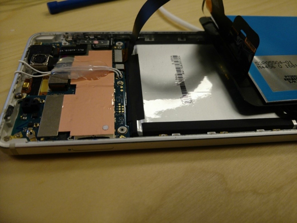
The steps were the following:
diffusing hot air on the surface of the telephone to melt the glue around the screen (this took over 30 minutes);
removing around 18 screws to access the board;
temporary solder to see if EDL mode could be accessed;
final solder where the EDL testpoints are linked through a push-button switch; if the switch is activated, the circuit closes and the testpoints are shortened, causing the bootROM to take the EDL boot path.
He also probed the board for UART pins (UART is extensively being used by the SBL), but, unfortunately, it seems like the UART port was removed on the phone we used.
Gaining Code Execution
This is extremely easy, even more so than on the Nexus 6P, because the pages at 0x08000000 are RWX. We thus uploaded the payload at this address and changed the return address (located at 0x0805CFDC).
Taking Over the Boot Chain
Once code execution is achieved, it is easy enough to take over the boot chain since both the bootROM and the programmer are Aarch32 code.
Taking Over the BootROM (PBL)
The bootROM is located and executes at address 0x00100000.
We adopted an approach similar to Aleph's here:
copy the bootROM in a buffer;
patch the copy;
remap the copy using the copy (the copy having appropriate patches to keep the address translation valid);
run the copy.
The patches are the following:
keeping the address translation mapping valid, ensuring the execution of the copy;
deactivating the testpoint check, so that the bootROM doesn't try to go to EDL over and over again;
injecting the SBL hook in the main function list.
Taking Over the SBL (secondary boot loader)
With the SBL hook injected into the bootROM copy, we made the following patches to the SBL:
deactivating secure boot (image verification and authentication) at the SBL level;
injecting the next QSEE (secure monitor) and aboot (Android bootloader) hooks;
Patching QSEE and Aboot, and Communicating with the PC
Once we have taken over the SBL, we can patch the Secure Monitor and aboot as they are loaded.
For QSEE, we added a hook on the "synchronous exception from lower Aarch32 exception level" exception vector. This allowed us to add an arbitrary EL3 read/write primitive accessed through the smc instruction.
On aboot side, the patches are the following:
implement a new fastboot command which exposes the abovementioned read/write primitive to the PC;
make it believe secure boot is disabled. This has the nice side-effect to make the bootloader unlockable with no unlock key needed.
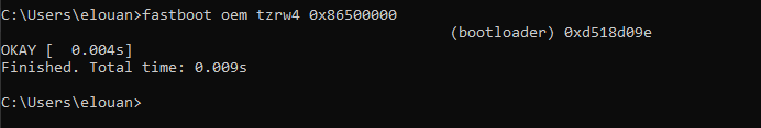
The end result is that we can read/write EL3 memory from fastboot while the system is running:
Studying the XPU Registers
Since we can now read/write EL3 memory, it is now finally possible to interact with the XPU registers, for which there is no public documentation whatsoever.
A particular function of the secure monitor, referencing "ERROR:MPU Partition overlapping found!", is the XPU fault handler and contains a lot of debug strings and information about the XPU registers.
List of hardware devices having XPU Units
The first thing that is easily noticeable is a big array of structure instances containing the names and addresses of the various XPU units on the Nokia 6.
The list is the following:
IPA_BAM_NDP, base XPU regs address at 0x7902000
IPA at 0x38000
A5X_XPU at 0x1C61000
Q6PCNOC_CFG at 0x32000
SDC1_SDCC_ICE at 0x7806000
LPASS_TOP at 0xC064000
TLMM at 0x1300000
TCU at 0x34000
QDSP at 0x37000
IMEM_MPU at 0x53000
GPS at 0x36000
MCDMA at 0x35000
BOOT_ROM at 0x1FF000
VENUS0 at 0x1DF0000
TCSR_REGS at 0x1936000
SEC_CTRL_APU at 0xAE000
RPM_APU at 0x287000
MSS at 0x4000000
MPM2 at 0x4A7000
CLK_CTL at 0x1880000
SNOC_CFG at 0x2D000
PCNOC_CFG at 0x2E000
PMIC_ARB at 0x200E000
WCSS_APU at 0xA21F000
DEHR at 0x4B0000
CRYPTO0_BAM at 0x702000
BAM_BLSP2_DMA at 0x7AC2000
BAM_BLSP1_DMA at 0x7882000
BIMC_MPU_0 at 0x44A000
XPU Register Structure
By looking at the function tables in the Secure Monitor pertaining to XPU registers, then reversing them, we have discovered most of the structure that all XPU units share.
Each XPU unit has the same kind of registers. Control registers make up the first 0x200 bytes, then there is a variable number of protection region registers set (each set being 0x80 bytes in size).
There are 3 sets of control registers (each being 0x80 in size), in this order: secure, nonsecure, and "MSS self-auth" (which purpose is still unknown to us). The first controls accesses made by the Secure World (including to the registers themselves), and the second accesses made by the Normal World.
typedef struct XpuControlRegisterSet {
    // Some regs are only in the secure block,
    // some others only in the nonsec block (like UMR_*, REV_*), some in both...
    u32 CR;                 // 0. "Control register"?
    u32 WDR;                // 4
    u32 PRTN_RACR_SHADOW0;  // 8. only for some types of devices (like BootROM)
    u32 unk_0c;
    u32 PRTN_START_SHADOW0; // 0x10. same
    u32 unk_14;
    u32 PRTN_END_SHADOW0;   // 0x18. same
    u32 unk_1c;
    u32 RPU_ACR0;           // 0x20
    unk_24, unk_28, unk_2c, unk_30, unk_34, unk_38, unk_3c;

    /* ============Error registers============ */
    u64 EAR0;               // 0x40
    u32 ESR;                // 0x48
    u32 ESRRESTORE;         // 0x4C
    u32 ESYNR0;             // 0x50
    u32 ESYNR1;             // 0x54
    u32 ESYNR2;             // 0x58
    /* =========End of error registers========= */

    u32 unk_5c;
    u32 UMR_RACR;           // 0x60
    u32 UMR_WACR;           // 0x64
    u32 unk_68, unk_6c;
    u32 UMR_CNTL;           // 0x70. nonsec only
    u32 IDR0;               // 0x74. sec only? "Interrupt Description Register 0"?
    u32 IDR1;               // 0x78. sec only? "Interrupt Description Register 0"?
    u32 REV;                // 0x7c
} XpuControlRegisterSet;

typedef struct XpuProtectionRegisterSet {
    u32 RACR0;              // 0x00
    u32 unk_4[7];
    u32 WACR0;              // 0x20
    u32 unk_24[7];
    u64 START0;             // 0x40
    u64 END0;               // 0x48
    u32 SCR;                // 0x50
    u32 MCR;                // 0x54
    u32 CNTL0;              // 0x58, only on some. Bit31: mpu partition disabled
    u32 CNTL1;              // 0x5C, same
    u32 unk_60[8];
} XpuProtectionRegisterSet;
An exhaustive list of all the XPU and their role can be found in the Annex section section of this blogpost.
Other XPU Findings
We can see in the annex that the control register has a reset deassert bit. One question that immediately comes to mind: if we keep an XPU unit in reset (e.g. the bootROM one), can we now do any kind of access to the affected unit?
The results are the following:
clearing the bit in the secure CR instance renders the XPU registers for the unit inaccessible;
clearing the bit in the non-secure CR instance makes all accesses from the normal-world stop causing faults, but data is read as 0, writes are ignored.
This means the XPU registers are only one mean to secure peripherals and/or memory, all of which can be protected by other technology like TrustZone isolation.
Conclusion and Acknowledgments
In a nutshell, I had the opportunity to work on two phones and gain a great understanding of the Qualcomm ecosystem overall.
Even though the work on the Nexus 6P stalled, I still had the opportunity to find interesting methods; on the Nokia 6, I have managed to read/write any memory while the system is running.
I would like to thank my internship tutors, Joffrey Guilbon (patate), Maxime Peterlin (lyte) and Alexandre Adamski (neat) for their precious help and guidance throughout my internship; as well as Guillaume Heilles (zours) for having "modded" the Nokia 6 phone I used.
I would also like to thank all my colleagues for the warm welcome I received, and for proofreading this article.
Bibliography
| [aleph] | Aleph Security, "Exploiting Qualcomm EDL Programmers (1): Gaining Access & PBL Internals", https://alephsecurity.com/2018/01/22/qualcomm-edl-1/ |
| [aleph2] | Aleph Security, "Exploiting Qualcomm EDL Programmers (2): Storage-based Attacks & Rooting", https://alephsecurity.com/2018/01/22/qualcomm-edl-2/ |
| [aleph3] | Aleph Security, "Exploiting Qualcomm EDL Programmers (3): Memory-based Attacks & PBL Extraction", https://alephsecurity.com/2018/01/22/qualcomm-edl-3/ |
| [aleph4] | Aleph Security, "Exploiting Qualcomm EDL Programmers (4): Runtime Debugger", https://alephsecurity.com/2018/01/22/qualcomm-edl-4/ |
| [aleph5] | Aleph Security, "Exploiting Qualcomm EDL Programmers (5): Breaking Nokia 6's Secure Boot", https://alephsecurity.com/2018/01/22/qualcomm-edl-5/ |
| [ROP] | Return-oriented programming, https://en.wikipedia.org/wiki/Return-oriented_programming |
| [TLB] | Translation lookaside buffer, https://en.wikipedia.org/wiki/Translation_lookaside_buffer |
| [Nokia6] | Nokia 6 wikipedia page, https://en.wikipedia.org/wiki/Nokia_6 |
| [Nexus6P] | Nexus 6P wikipedia page, https://en.wikipedia.org/wiki/Nexus_6P |
| [QualcommSB] | Qualcomm, Secure Boot and Image Authentication Technical Overview, https://www.qualcomm.com/media/documents/files/secure-boot-and-image-authentication-technical-overview-v1-0.pdf |
| [SoCs] | System on Chip, integrated circuit integrating all the basic components a system needs: CPU, memory, many peripherals, etc. |
| [OTA] | Full OTA Images for Nexus and Pixel Devices, https://developers.google.com/android/ota |
| [firehorse] | https://github.com/alephsecurity/firehorse |
Annex
XPU Registers Description
Legend:
S = "Secure"
NS = "Non Secure"
RESn = "Reset to n"
CR: Control Register, offset 0x00
| Bits | Description |
|---|---|
| 31-17 | RES0, RO |
| 16 | S: RES0, RO NS: ? RW |
| 15-11 | RES0, RO |
| 10-9 | ? |
| 8 | Enables something |
| 7 | RES0, RO |
| 6 | S: ? NS: RES0, RO |
| 5 | S: RES1, RO NS: RES0, RO |
| 4 | RES1, RO |
| 3-1 | ? |
| 0 | Reset deassert |
Writing 0 to the "XPU unit enable" bit of the secure version of the register (SCR) causes access faults when later accessing the register for this XPU unit, even if the access was made from the Secure World.
EAR0: Error Address Register 0, offset 0x40
Contains the physical address of the fault.
ESR: Error Status Register, offset 0x48
| Bits | Description |
|---|---|
| 31 | "Multiple" fault |
| 30-4 | RES0, RO (?) |
| 3 | ? |
| 2 | ? |
| 1 | "Client" fault |
| 0 | "Config" fault |
ESRRESTORE: Error Status Register Restore (?), offset 0x4C
Used to acknowledge and clear errors. Writes to this registers are copied to ESR (maybe?).
ESYNR0: Error Synthesis Register 0, offset 0x50
| Bits | Description |
|---|---|
| 31-24 | TID |
| 23-16 | VMID |
| 15-13 | BID |
| 12-8 | PID |
| 7-0 | Master ID |
| 0 | "Config" fault |
ESYNR1: Error Synthesis Register 1, offset 0x54
| Bits | Description |
|---|---|
| 31 | ERROR_DCD fault |
| 30 | ERROR_AC fault |
| 29 | Addr. read-allocate flag |
| 28 | Addr. burst flag |
| 27 | Addr. "exclusive" flag |
| 26 | Addr. write flag |
| 25 | Addr. "full" flag |
| 24 | Addr. read "BEADNDXEN" flag |
| 23 | Addr. out-of-order flag |
| 22 | ? |
| 21-19 | "pReqPriority" |
| 18-16 | "Size" |
| 15 | Addr. "MSS SELF AUTH" flag |
| 14-8 | "Length" |
| 7 | Addr. "instruction" flag |
| 6 | Addr. prot. is NS flag |
| 5 | Addr. private flag |
| 4 | Addr. inner-shared flag |
| 3 | Addr. shared flag |
| 2-0 | Memory type |
ESYNR2: Error Synthesis Register 2, offset 0x58
| Bits | Description |
|---|---|
| 31-4 | ?, RES0? |
| 3 | Save/restore in progress |
| 2 | MSA region match |
| 1 | Secure region match |
| 0 | Nonsecure region match |
IDR0: Interrupt Description Register 0, offset 0x74
?
IDR1: Interrupt Description Register 1, offset 0x78
| Bits | Description |
|---|---|
| 31-11 | ? |
| 10 | 0 for faults |
| 9-0 | ? |