Author Gwaby
Category Exploitation
Tags AMD, Steam Deck, vulnerability, UEFI, SMM, 2025
In this blog post we explain the consequences of asking our R&D boss for a Steam Deck as a Christmas gift. It involves a couple of vulnerabilities, limited primitives, challenging exploitation and a long disclosure process.
Introduction
Serious Story
This blog post aims to showcase a couple of bugs affecting Valve's Steam Deck and generally various devices running on AMD. Some of the primitives induced by these bugs are very limited and offer a good playground to work on exploitation techniques.
Context
Go directly to the technical details if you want to skip useless rambling.
The idea of this research started around December 2023, right in the timeframe when you need to rush and buy gifts because you're too lazy to hunt for them in advance. As a pure matter of coincidence, this timeframe matched the release of the new OLED version of the Steam Deck.
For non-gamer readers, Valve's Steam Deck is a small handheld PC specifically designed to let people play wherever they want. It embarks a custom AMD APU, dubbed Van Gogh, based on the Zen 2 microarchitecture. Its operating system, SteamOS 3.0, is a modified version of Archlinux that runs on a read-only file system (except for a few writable directories). On top of that lies Proton, a piece of software that provides the compatibility layer needed for games developed for Windows to run on the device. Basically, that's just a cool tiny gamer PC shaped as a portable console.
As a couch potato princess with a substantial Steam library (and no clue about what to offer to friends and family), it was not that long before the dilemma arose between either disappearing with a new shiny toy for a month or behaving as a socially adapted person and enduring this dreadful period.
While both possibilities could appear tempting, a third one was eventually devised after a lot of pondering: try to push someone to buy the device and test it after Christmas (and also find proper gifts too).
And since "mastermind" is definitely not a skill in the regular gears of a couch potato, the most straightforward way is to bluntly ask the company to acquire it.
Long story short, the response was: "Okay, finish your current mission, pwn it and bring us some cool R&D".
Setup
As our main topic of interest at the moment is UEFI, we exclusively focused on the Steam Deck bios for this research.
Retrieving the firmware is very easy and can be done in various ways.
Since it is built from Insyde's code base, the most straightforward method is to simply dump the SPI flash with the vendor's flashing utility:
sudo /usr/share/jupiter_bios_updater/h2offt /home/deck/biosbkp.fd -O
Alternatively, another good solution is to download the last version from the unofficial public repository on gitlab.
The images labeled as F7A0* are for the LCD model, while the F7G0* ones are related to the OLED version.
Finally, if for some reason both previous ways didn't work out, the SPI chip (Winbond W25Q128JW) is accessible in the back of the Steam Deck and can be read with a chip programmer. For the record, iFixit teams published a detailed teardown that can be a great source of information for people wanting to poke the hardware.
With the firmware at hand, extracting and analyzing the modules is a child play with UEFITool and EfiXplorer.
Another great tool to have is EfiPy. This small library can be compiled, alongside chipsec, with Python368.efi and greatly helps prototyping PoC from the UEFI Shell.
With this, we're ready to start playing around with our target.
Technical details
If you're not familiar with the UEFI ecosystem, we recommend to start with the first part of this blog post about a tiny bug in EDK2 implementation, or even better dig into Tianocore's white papers.
That said, two vulnerabilities[*] were identified in the UEFI firmware running on the Steam Deck. Both of them are the consequence of improper data validation issues. For this blog post, we will mainly focus on only one of them as it is the most interesting to explain and exploit.
While impacting multiple families of devices, we will solely focus on the Steam Deck here. The provided offsets match the binaries in the bios version F7A0120.
[*] Actually there is a third one that was not patched in Valve's build, but since it is already known (CVE-2022-35894, CVE-2022-35895, CVE-2021-33627), we won't speak about it in this blog post.
The Vulnerabilities
Bug #1 - AmdPspP2CmboxV2.efi (CVE-2024-21925)
The first bug, located in AmdPspP2CmboxV2.efi (4759E93E-8F44-448F-88A1-BD97FC47BEA5), is very straightforward and can be summarized as a lack of validation in the parameters sent to the SMM communication handler.
This handler (offset 0x26D0) expects the following structure as buffer input:
// Handler GUID: B2ABCCBF-02E1-436F-98B020599C49E2A1

struct Comm_Buffer {
    /*000*/ UINT32 cmd_id;
    /*004*/ UINT8  psp_cmd;
    /*008*/ UINT64 arg0;
    /*010*/ UINT64 arg1;
    /*018*/ UINT64 arg2;
    /*020*/ UINT64 arg3;
}
The cmd_id field determines the action the module should perform:
- 1: Get information related to the flash regions.
- 2: Read flash region;
- 3: Write flash region;
- 4: Erase flash region;
- 5: Unregister handler;
- 6: Send data to the PSP;
- 7: Retrieve data from the PSP;
While the communication buffer is verified, the parameters inside the structure are, in some cases, not. Therefore, several commands can be used to leak or tamper with the SMRAM.
As an example, the id 2, responsible for reading and returning flash regions ensures that the destination (represented with arg0 as its address and arg1 as its size) is valid but does not enforce such check on the source address (arg2), leading to data leak from SMRAM.
The commands 3 and 4, used to write and erase a flash region, are prone to the same issue. However, due to some restrictions in the underlying module,FwBlockServiceSmm.efi, in charge of updating the firmware, it is not possible to easily overwrite the SMRAM.
The commands 6 and 7 are used to communicate with the Platform Security Processor through a mechanism of mailboxes. Here again, the parameters are not sanitized enough: by providing an address in SMRAM as a response buffer (arg2), an attacker can overwrite data in SMM with PSP answers.
It should be noted that, this handler is removed before entering the Run Time phase, when AmdPspDxeV2Ff3.sys executes its notification routine for the EFI_EVENT_EXIT_BOOT_SERVICES_GUID event.
Therefore, one must have physical access to the device to reach the vulnerability, which can appear rather inconvenient in some contexts. Still, to experiment with the Steam Deck, this is a neat capability to have.
Bug #2: AmdCpmDisplayFeatureSmm.efi (CVE-2024-0179)
The second vulnerability lies in an SMM module called AmdCpmDisplayFeatureSmm.efi (30AF4110-A58E-4EF7-8C75-B725939B3B9F). As the name suggests, this module seems related to a hardware device: the CCIX-PCIe Module (CPM). We won't go too far in the explanation, but a bit of googling presents the Cache Coherent Interconnect for Accelerators standard, or CCIX, as a technology providing cache-coherent shared memory across hardware components.
Two other UEFI modules mainly interact with AmdCpmDisplayFeatureSmm.efi: its DXE counterpart named AmdCpmDisplayFeatureDxe.efi, and another one in SMM called AmdCpmInitSmm.efi. The three of them appear to be used to initialize and provide information from/to the CPM.
AmdCpmDisplayFeatureSmm.efi registers two software SMI (SWSMI):
- a handler with the ID 0xE3 and located at offset 0x3364;
- a handler with the ID 0xED and located at offset 0x3488;
The whole process involved in these handlers is quite complex and won't be described in this post.
The functions relevant in the context of the vulnerability are at offset 0x2304 (called by the handler 0xED) and 0x280C (called by the handler 0xE3) in the vulnerable module.
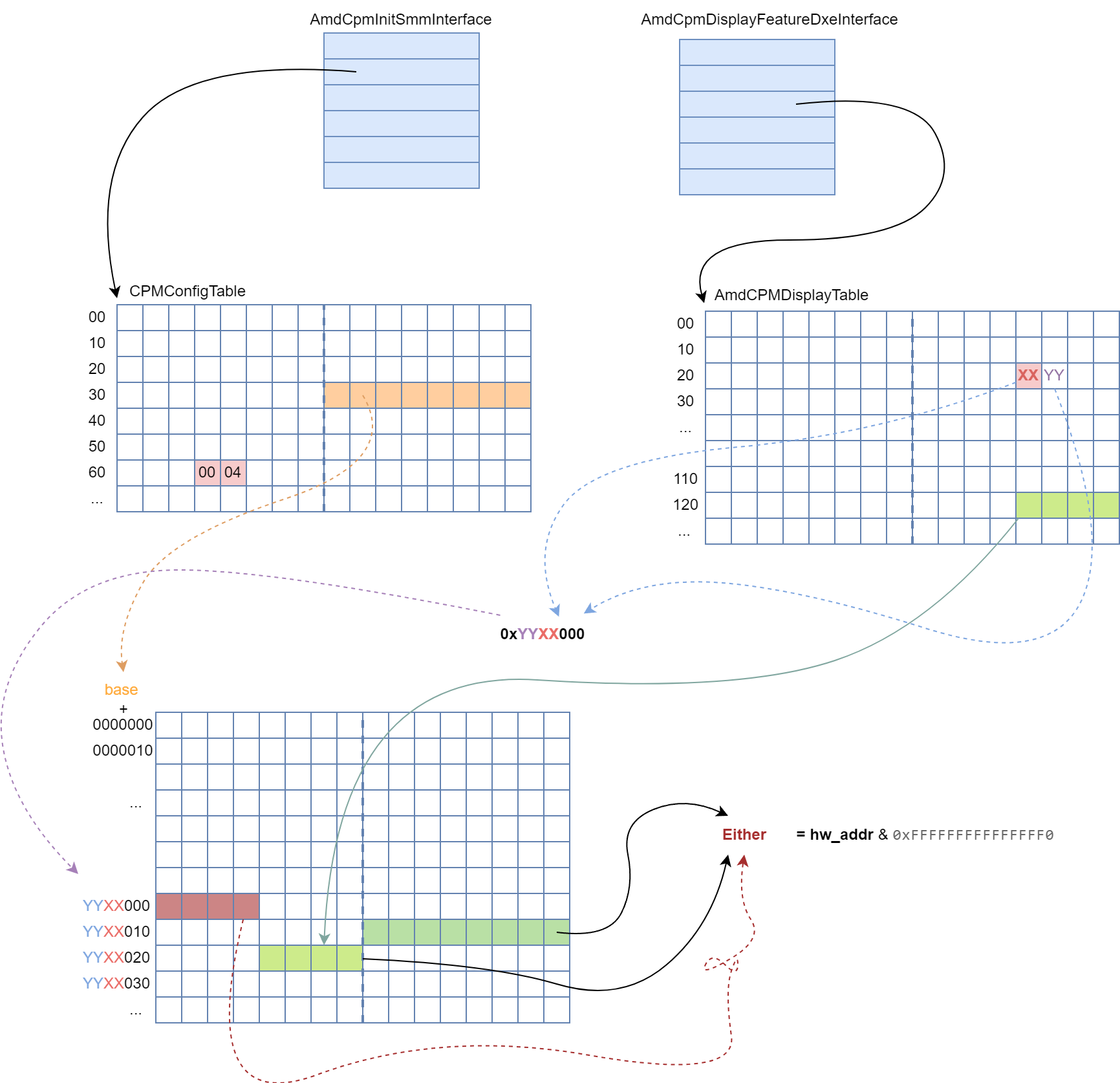
They rely on the information provided by AmdCpmDisplayFeatureDxe.efi and on a data array, dubbed CPMConfigTable in this post, which is accessible through AmdCpmInitSmm.efi interface. These elements are located in DXE and are used to compute offsets and addresses in the memory space of what seems to be the CPM.
As an example, the computation for function 0x2304 can be summarized with the following code:
UINT8 *CPMConfigTable = (UINT8 *)(AmdCpmInitSmmInterface + 8);
UINT8 *AmdCpmDisplayTable = (UINT8 *)(AmdCpmDisplayFeatureDxeInterface + 0x10);

if(*(UINT16*)&CPMConfigTable[0x63] != 0x400 || AmdCpmDisplayTable[0x2c] == 0){
  return;
}

UINT8 val_2c = AmdCpmDisplayTable[0x2c];
UINT8 val_2d = AmdCpmDisplayTable[0x2d];
UINT32 value = AmdCpmInitSmmInterface.readDwordFromAddress(val_2d, val_2c >> 3, val_2c & 7, 0);
AmdCpmInitSmmInterface.writeDwordToAddress(val_2d, val_2c >> 3, val_2c & 7, 0x24, AmdCpmDisplayTable[0x12c])

// ...
value = value >> 0x10;
UINT32 temp = 0;
if(value <= 0x67C0)
  temp = 0x10;
else if(value <= 0x67E0)
  temp = 0x11;
// ...
else if(value <= 0x7420)
  temp = 0x28;

if(temp != 0){
  hw_addr = AmdCpmInitSmmInterface.readDwordFromAddress(val_2d, val_2c >> 3, val_2c & 7, 0x24);
}else{
  hw_addr_hi = AmdCpmInitSmmInterface.readDwordFromAddress(val_2d, val_2c >> 3, val_2c & 7, 0x1c);
  hw_addr_low = AmdCpmInitSmmInterface.readDwordFromAddress(val_2d, val_2c >> 3, val_2c & 7, 0x18);
  hw_addr = (hw_addr_hi << 0x20) | hw_addr_low;
}
  hw_addr &= 0xFFFFFFFFFFFFFFF0;
  if (temp > 0x20)
    hw_addr[0x34E0] &= 0xEFFFFFFF;
  else if (temp > 0x10)
    hw_addr[0x540C] &= 0xFFFFEFFF;
  else
    hw_addr[0x5418] &= 0xFFFFFFFD;
// ...
where readDwordFromAddress and writeDwordToAddress are provided by AmdCpmInitSmm.efi and can be described as follows:
UINT32 readDwordFromAddress(UINT8 high, UINT8 middle, UINT8 low, UINT8 offset){
    UINT64 base = *(UINT64*)&CpmConfigTable[0x33];
    UINT32 *addr = (high << 0x14) + (middle << 0xf) + (low << 0xc) + offset + base;
    return *addr;
}

UINT32 writeDwordToAddress(UINT8 high, UINT8 middle, UINT8 low, UINT8 offset, UINT32 value){
    UINT64 base = *(UINT64*)&CpmConfigTable[0x33];
    UINT32 *addr = (high << 0x14) + (middle << 0xf) + (low << 0xc) + offset + base;
    *addr = value;
}
The process in the function at offset 0x280C is quite similar but involves different offsets and values. Furthermore, the final operation differs from the logical AND shown above:
// ...

hw_addr = AmdCpmInitSmmInterface.readDwordFromAddress(val_2d, val_2c >> 3, val_2c & 7, 0x24);
hw_addr &= 0xFFFFFFFFFFFFFFF0;
if (temp > 0x20){
  hw_addr[0x5780] &= 0xFFFFFFFD;
}
else if (temp > 0x10){
  hw_addr[0x53F4] &= 0x0FFFFFF00;
  hw_addr[0x53F4] |= 0x83;
}
  // ...
As both AmdCpmDisplayFeatureDxe.efi interface and CPMConfigTable table are located in DXE, it is possible to modify their content and change the value of hw_addr to an address in SMRAM. This leads to the possibility for an attacker to gain two primitives:
- arbitrary logical
ANDwith a mask of either0xEFFFFFFF,0xFFFFEFFFor0xFFFFFFFD, depending on the address alignment; - arbitrary write of 1 bytes (
0x83) at addresses having the lowest nibble equal to 4.
For the astute reader that is currently screaming in indignation as to why the call to writeDwordToAddress is not presented as an easy peasy way to gain our write primitive, it's not because we somehow missed it, but simply due to the destination address being overwritten several times in the very long and omitted computation that happens before, in-between and after the presented snippet. Relying only on the aforementioned AND and OR operations are less prone to unforeseen side effects.
Anyway, although these primitives are quite limited, it is still possible to transform them to arbitrary read and write in SMRAM, and ultimately code execution.
Side Note - Reaching the bug
As it was explained previously, the vulnerable handlers in AmdCpmDisplayFeatureSmm.efi are accessible through two SWSMIs. Unfortunately, if one tries to blindly trigger them with the usual write access to the I/O port 0xb2, such as what chipsec does, it results in, well, nothing. :)
The reason is simple: the I/O port responsible for that is different.
The following snippet comes from the Trigger function in AmdSmmControl.sys DXE module, which is called by PiSmmIpl.sys to send an SWSMI when using the EFI_SMM_COMMUNICATION_PROTOCOL protocol:
; __int64 Trigger(void *this, int *commandPort, int *dataPort, int periodic, int activationInterface)
Trigger proc near
; ...

movzx   edx, cs:io_port
mov     ecx, 100h
movzx   eax, r10b       ; dataPort
imul    eax, ecx        ;    data: XX00
movzx   ecx, bl         ; commandPort
add     ax, cx          ;    cmd: 00XX
out     dx, ax
; ...
The io_port global variable is initialized with a value obtained from the Power Management Registers (0xCD6/0xCD7) during the driver init:
mov     r9d, 0CD6h
lea     r10d, [r9+1]
; ...
mov     edx, r10d
in      al, dx
mov     cs:io_port, al
A small EFI script enables to extract the content of this variable (quick and dirty style):
from EfiPy import *

gEfiSmmControl2Guid = \
    EFI_GUID(0x843DC720, 0x0AB1E, 0x42CB, (0x93, 0x57, 0x8A, 0x0, 0x78, 0x0F3, 0x56, 0x1B))

Interface = PVOID()
Status = gBS.LocateProtocol(
    byref(gEfiSmmConfigurationProtocolGuid),
    None,
    byref(Interface)
)
if Status:
    print("LocateProtocol() failed: 0x%016x" % Status)
    exit()

SmmControlInterface_ofst = 0x21B0
SmmIOPort_ofst = 0x2204

AmdSmmControl_base = Interface.value - SmmControlInterface_ofst
print("AmdSmmControl = 0x%x" % AmdSmmControl_base)

Ioport_addr = AmdSmmControl_base + SmmIOPort_ofst
IoPort = cast(Ioport_addr, POINTER(UINT8)).contents.value
print("IO Port = 0x%x" % IoPort)
Which results in:
FS1:\EFI\Tools\> Python368.efi get_ioport.py
AmdSmmControl = 0x78efe000
IO Port = 0xB0
A regular client wishing to communicate with an SMM handler on runtime can also legitimately get this value from the Fixed ACPI Description Table (FADT) at offset 0x30.
Exploitation
In this section, we will see how to leverage the second bug (in AmdCpmDisplayFeatureSmm.efi) to gain code execution in SMM on runtime.
AND Mask to Arbitrary Read Primitive
As we already saw, AmdPspP2CmboxV2.efi provides the capabilities to totally leak the SMRAM. The issue is that the handler can solely be reached in DXE as it is unregistered before starting the Run Time phase. Therefore, the other vulnerability, in AmdCpmDisplayFeatureSmm.efi, must be employed to regain such primitive from the main OS.
Also, to be totally honest, one personal hidden achievement for this research was to exploit the target only using the AND operations from the handler 0xED. Unfortunately, as a down-to-earth coworker said, only puzzle game nerds would be interested in a walk through that deliberately omits an easier path just for the love of the challenge, so we stopped being a thick head after achieving the arbitrary read primitive.
What can be controlled?
As it was described in the vulnerability section, exploiting the handler with ID 0xED can provide a limited AND primitive.
Two conditions must be met in order to reach the interesting piece of code:
- The byte at offset 0x2C in
AmdCpmDisplayTablemust be non-null; - The 11th bit (bit 10) of the value at offset 0x63 in
CPMConfigTablemust be set;
The computation to determine the destination address, described in the previous piece of code, can be summarized as:
"You take the base address in one table and the page number in another, it gives you the address of a value. This value determines where the destination address will be retrieved. Beware, in one case, the latter actually comes from the second table. Anyway, a bit mask is applied on it to be sure it is aligned and then, you add hardcoded offsets and voila".
Or with a picture:
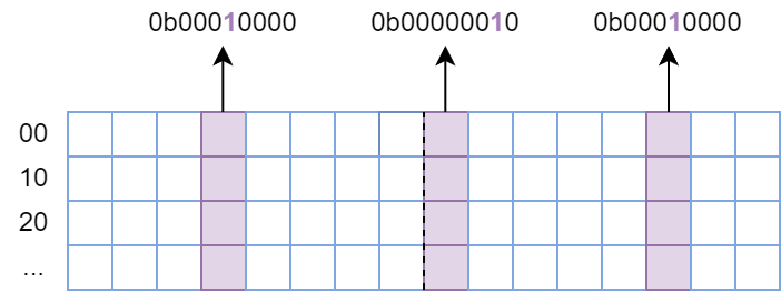
While being a bit messy, the final control we gain over the memory is that we can erase one bit at this address plus the following offsets:
- Offset 0x34E0 (bit mask 0xEFFFFFFF) -> clear bit 0x1c;
- Offset 0x540C (bit mask 0xFFFFEFFF) -> clear bit 0xc;
- Offset 0x5418 (bit mask 0xFFFFFFFD) -> clear bit 1;
As the lowest nibble of the address is zeroed before adding the offsets, the final destination cannot be shifted and has to be aligned on a 10-byte boundary.
It basically means that we control (or at least we can erase) the following bits:
What Could Be Tampered?
Knowing what can be affected, we simply need to find where this can have a useful impact.
For this, another SMM module present in the Steam Deck will be leveraged: IhisiServicesSmm.sys. Please note that this module is provided by Insyde and may not be available on other AMD-based platforms.
IhisiServicesSmm.sys's SWSMI handler is interesting in the context of (post-)exploitation as it provides a way to register and call commands capable of performing various tasks. Among these, we can find classical operations such as manipulating non-volatile variables, obtaining information about the platform, or reading and writing flash memory, but also others related to OEM components and mechanisms.
These commands are identified by IDs and can be called by providing these to the IOdata port. Commands involved in the same process are labeled with the same ID, meaning that for one SWSMI triggered, multiple commands can be executed. Their running order is determined with a mechanism of priority. It should be noted that if an error occurs during the execution of the group of commands, the process stops and the error is returned to the client as a status code.
Data transferred to and from the commands are either passed via the registers or in a shared memory whose address and size can be requested to the module with the command ID 0x83.
For a request to be considered as valid, RBX must hold the $H2O magic. The content of the other registers are command-dependent.
Commands manipulating memory usually employ two functions to ensure that the provided addresses are valid depending on the context:
- One ensuring that the address is within the boundaries of the shared memory (dubbed
IsSharedBufferValidin this blog post); - One checking whether the address is inside SMRAM or not (simply named
IsInSmRam).
IsInSmRam is a very simplified version of SmmIsBufferOutsideSmmValid API:
BOOLEAN IsInSmRam(EFI_PHYSICAL_ADDRESS buffer, UINT64 length){

    EFI_PHYSICAL_ADDRESS end_buffer = buffer + (length - 1);
    if(buffer == 0 || length == 0)
        return FALSE;

    if(end_buffer < buffer)
        return TRUE;

    for (Index = 0; Index < mSmmIhisiSmramCount; Index++) {
        if ((end_buffer >= mSmmIhisiSmramRanges[Index].CpuStart) &&
            (Buffer < mSmmIhisiSmramRanges[Index].CpuStart + mSmmIhisiSmramRanges[Index].PhysicalSize))
            return TRUE;
    }

        return FALSE;
}
To bypass this check, the most obvious way would be to put mSmmIhisiSmramCount to 0.
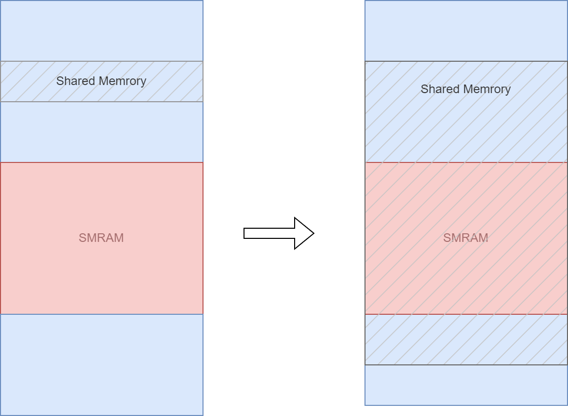
Thankfully for us, the stars are somewhat aligned: in our firmware, mSmmIhisiSmramCount global variable is located at offset 0xF318 in the module. Furthermore, the SMRAM range table holds only two entries: one for the very first page of the SMRAM, another for the remaining regions.
Therefore, tweaking this variable with the AND capability (using offset 0x5418 with the bit mask 0xFFFFFFFD) would totally erase the variable. [*]
(For the same astute reader that screamed previously in indignation and is now ranting about how unoriginal this technique is: yes, you're right, this is the very same idea as what was presented in the previous blog post but with another type of primitive).
With this check bypassed, gaining a read primitive is trivial: one just need to call the operation in charge reading the flash (ID 0x14).
Data are provided through the following parameters:
- RCX: size;
- RSI: output buffer;
- RDI: source address;
Reading the flash is performed via three different commands:
S14Cs_DoBeforeRead0: priority level 0xE0 (offset 0x5888);S14Kn_FbtsReadProce: priority level 0x80 (offset 0x685C);S14Cs_DoAfterRead00: priority level 0x20 (offset 0x5950);
We won't go into the details of their implementation, however it should be noted that the parameters are verified before being processed: the source address should not be within the SMRAM range (IsInSmRam) and the destination must be in the shared memory boundaries (IsSharedBufferValid).
As we removed the purpose of IsInSmRam, any source address is considered as valid and the handler will gladly write its content back to the shared buffer.
[*]: Actually, since the handler 0xE3 also provides the possibility to apply the same 0xFFFFFFFD bit mask on addresses aligned on a 0x10-byte boundary, it would still be possible to exploit the targeted variable should it be shifted elsewhere in memory.
1-Fixed Byte Write to Arbitrary Write Primitive
While we leveraged the command responsible for reading the flash in order to gain a read primitive in SMRAM, one can hardly do the same with its write counterpart. Indeed, both read and write mechanisms rely on the same "backend" as AmdPspP2CmboxV2.efi (FwBlockServiceSmm.efi). Thus, the command suffers from the same kind of limitations as what was presented previously, and it is rather tedious to leverage it to gain our write primitive.
Still, using this specific command is not needed as long as we bypass the second validation of the read one.
As we described previously, the destination buffer for this command is verified with IsSharedBufferValid function, which can be summarized as:
BOOLEAN IsSharedBufferValid(EFI_PHYSICAL_ADDRESS buffer, UINT64 length){

    EFI_PHYSICAL_ADDRESS end_buffer = buffer + (length - 1);
    if(buffer == 0 || length == 0 ||
        end_buffer < buffer       ||
        buffer < mIhisiCommandBuf ||
        end_buffer > mIhisiCommandBuf + mIhisiCommandBufSize)
        return FALSE;

            return TRUE;
}
Here, solely relying on the AND capabilities is not possible as both mIhisiCommandBuf and mIhisiCommandBufSize are aligned on a 0x10-byte boundary and the bit mask won't affect them. Thus the second primitive (1-fixed byte write) must be employed.
As we saw previously, this primitive offers the possibility to write 0x83 at any address which has the lowest nibble equal to 4. This is somewhat restrictive but still perfect to get rid of the check in this specific context.
mIhisiCommandBufSize being a 64-bit long variable, overwriting its highest bytes enables to extend the shared buffer far enough to overlap it with the SMRAM.
From this point, any address in SMRAM is considered by IsSharedBufferValid within the boundary of the shared memory and thus is valid.
Arbitrary Read-Write Primitive to Code Execution
To achieve code execution in SMM, one could simply create a fake SWSMI handler as it was described in the previous blog post.
However, in order to entertain our astute reader, we'll try something a tiny bit different. Here again, this method will only work if the firmware is based on Insyde's project as we leverage IhisiServicesSmm's interface. Since the module was already used to gain previous primitives anyway, we hope our hot-headed reader won't complain too much about the technique not being generic at this point.
Ihisi commands can be dynamically added and removed via IhisiServicesSmm's interface:
struct EFI_SMM_IHISI_PROTOCOL {
    UINT64                  Size;
    IHISI_ADD_IHISI_CMD     AddIhisCmd;        // add new command
    IHISI_REMOVE_IHISI_CMD  RemoveIhisCmd;     // remove commands
    IHISI_CALL_CMD_GROUP    CallCmdGroup;
    IHISI_READ_SAVE_STATE   ReadSaveState;
    IHISI_WRITE_SAVE_STATE  WriteSaveState;
    IHISI_IS_IN_SMRAM       IsInSmRam;
    IHISI_IS_BUFFER_VALID   IsBufferValid;
    IHISI_GET_AUTH_STATUS   GetAuthStatus;
    IHISI_GET_CMD_BUFFER    GetCmdBuffer;
    IHISI_UNKNOWN           GetUnknownBuffer;
    IHISI_IS_UNKN_BUF_VALID IsUnkBufValid;
    IHISI_CALL_COMMAND      CallCommand;
}


typedef EFI_STATUS (EFIAPI *IHISI_ADD_IHISI_CMD) (
  UINT32                     CmdId,
  IHISI_FUNCTION             Function,
  UINT8                      Priority
);

typedef EFI_STATUS (EFIAPI *IHISI_REMOVE_IHISI_CMD) (
  UINT32                     CmdId,
  UINT8                      Priority_min,
  UINT8                      Priority_max
);
In order to keep track of what was registered, the module holds a double linked list of objects representing each command.
struct EFI_SMM_IHISI_CONTEXT {
    UINT32                   Signature;         // 'SIHI'
    EFI_SMM_IHISI_PROTOCOL   IhisiInterface;
    LIST_ENTRY               CmdList;          // IHIS_COMMAND_GROUP objects list
    UINT64                   CpuIndex;
    EFI_SMM_CPU_PROTOCOL     SmmCpuInterface;
}


struct IHIS_COMMAND_GROUP {
    UINT64     Signature;                 // 'SIHI'
    LIST_ENTRY CmdList;
    UINT64     CmdId;
    LIST_ENTRY HandlerList;                //   IHIS_API_LIST_ENTRY objects list
};

struct IHIS_CMD_HANDLER {
    UINT64     Signature;
    LIST_ENTRY HandlerList;
    UINT64     Handler;
    UINT64     PriorityLevel;
}

/*
For the very nitpicking astute reader, yes, the source code for this module was leaked few years ago. These snippets are coming from my understanding of the mechanism, though, so they may not be the exact translation of the original code.
*/
Or in a more graphical way:
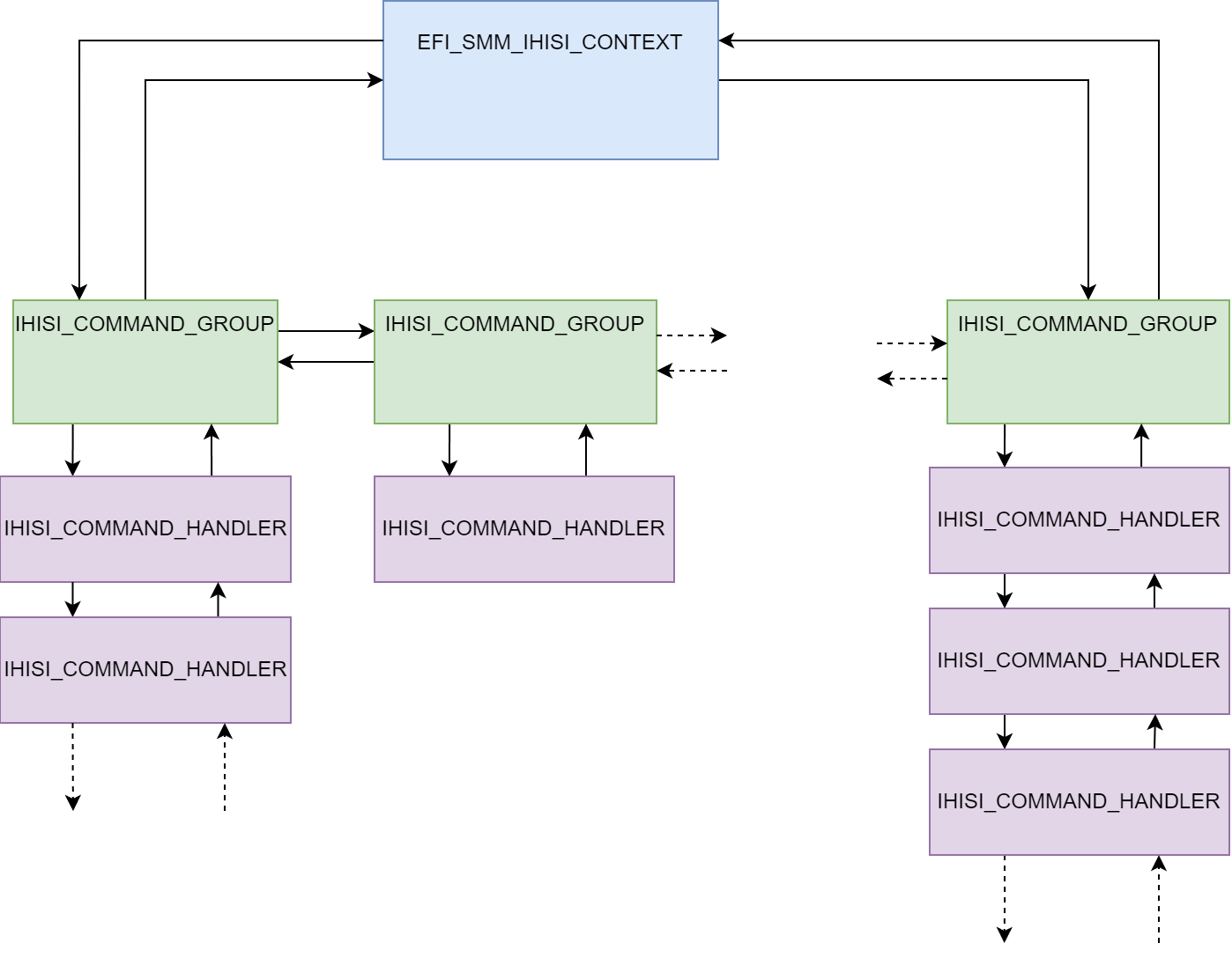
To gain code execution, one might craft a fake command and add it to the double linked list of aforementioned objects. As Insyde provides a legitimate driver for clients wishing to execute commands on runtime, the communication vector needed to interact with our rogue handler is already provided, which is pretty handy for lazy couch potatoes.
The shared memory used by the mechanism is rather big and most of the registered commands don't even use half of it. Therefore, it is possible to use it to put everything needed to execute the first stage in the exploitation process.
Unfortunately, in UEFI, memory access protection is enforced at the page table level and those tables are write-protected. The communication buffer, as well as all pages allocated as EfiRuntimeServicesData, are not executable, meaning that it is not possible to execute code directly from them.
To make a RW page executable, one needs to swap the write protect bit in the CR0 register and clear the NX bit for the page entry corresponding to the targeted page address.
This can easily be done via a small ropchain. While we won't go into the tiny details of its implementation, the gist is the following:
- Step 0: Overwrite an object (for an unused handler) to craft a fake stack and redirect to the ropchain in shared memory;
- Step 1: Get the PML4 value and allocate a new buffer;
- Step 2: Go through the page table entries and remove the NX protection for the buffer;
- Step 3: Clean the object that was used for the stack pivot and write the fake handler;
With this, we gained our exploitation primitive. Victory!!
Post-Exploitation
Okay, cool story. But what can we actually do with this new handler? For now, even though we're overlords on the machine (kind of), the handler is only capable of executing code in SMM, which is cool but a bit too restrictive to consider the target totally wrecked.
As a matter of fact, even though the SMM mode can interact with the entire physical memory, it runs in huge real mode making access to the OS unpractical.
In order to read or write data in the context of the OS (kernel or userland), one needs to do some gymnastics. The process is to go through the OS page tables entries to resolve the virtual addresses while ensuring that each and every physical page we use are mapped in SMM before accessing it.
If the physical page is present, the process is straightforward and nothing much needs to be done, however, if it's not, we have to map it ourselves. As it's rather stupid to try and reinvent the wheel instead of reusing smart techniques, we'll just copycat Dmytro Oleksiuk's ideas from his SMM backdoor.
Without paraphrasing him, the gist of his technique is to tamper with the page table entry of the first page in SMRAM to make it point to the one to remap. This way, reading or writing data in the first page will instead affect the targeted one.

And voila. With a bit of engineering, we can build a useful tool to monitor everything that runs on the machine in a transparent way for the OS (well, except when poping a calc, of course).
For the astute reader that is wondering why the demo showcases a Windows OS instead of the regular SteamOS: it's just a question of preferences for the post-exploitation part.
Conclusion
In this blog post, we presented two bugs that impact many devices running on AMD: one in AmdCpmDisplayFeatureSmm.efi accessible through the SWSMIs 0xED and 0xE3, and the other in a communication buffer provided to AmdPspP2CmboxV2.efi SMM driver. Both of them are the result of a lack of validation on the data used by the handlers in their respective processes.
These vulnerabilities can be leveraged to gain code execution in SMM either via the DXE phase or on runtime. The primitives induced by them are somewhat restrictive, but rather neat to transform, making our target, the Steam Deck, a good playground in another way than the one initially intended by its creators.
Acknowledgement
Many thanks to the R&D team for approving this silly research without questioning my dubious motivations (and especially to Ivan for handling the disclosure process). Also, kudos to Pauline for being a cool and understanding manager. ;)
Thumbs-up to Thierry for challenging my reasoning and to all the proofreaders that work hard to enhance the quality of this blog.
And last but not least, many many thanks to Mengsi and Eloïse for the cute phone holder that also fits surprisingly very well the Steam Deck. You rock, girls!
Disclosure timeline
Below we include a timeline of all the relevant events during the coordinated vulnerability disclosure process with the intent of providing transparency to the whole process and our actions.
- 2024-07-06 Quarkslab sent a report of the vulnerabilities to AMD PSIRT, publication deadline is set to October 1st, 2024
- 2024-07-08 AMD PSIRT acknowledged the report and assigned internal IDs (SWSPLAT-455, SWSPLAT-613) to track them. The vendor stated that the proposed deadline would not be viable and asked if it could be extended.
- 2024-07-26 AMD said they were still analyzing the issues and asked for a reply to their request to extend the disclosure deadline.
- 2024-07-30 AMD informed that their teams had reviewed the vulnerabilities and determined that the fix for one of them would require a system reboot and noted that data center customers are reluctant to such fixes. They proposed August 12th, 2025 as disclosure date to give customers time to deploy fixes.
- 2024-08-01 Quarkslab replied that the vulnerabilities were part of a research project that had to be published before the end of 2024 and the proposed embargo period of more than one year since the initial report was not acceptable. Noted that Quarkslab and its customers are AMD customers too. Quarkslab said it did not consider reasonable the request to keep its customers uninformed about the risk to their compute infrastructure because some other AMD customers have longer patch deployment schedules and are sensitive about reboots. Quarkslab said it was willing to extend the embargo period to 120 days since initial report (which is a reasonable upper bound) provided that AMD gave an status update and actual estimated date for the release of patches.
- 2024-08-12 AMD provided a status update. Both vulnerabilities were being fixed and their estimated release date was December 10th, 2024. The vendor explained that once the patches are shared with customers, some of them expect 3-4 months to triage, integrate, test the fixes and prepare their disclosures/security advisories and Quarkslab proposed 120-day embargo period would set the disclosure date to November 4th, 2024, which doesn’t give AMD customers enough room.
- 2024-08-15 AMD provided a status update. The release date for fixes could be advanced to October 21st, 2024. Therefore they proposed February 11th, 2025 as disclosure date. That would give AMD customers enough time to integrate, test and deploy them. AMD offered to discuss the matter in a conference call.
- 2024-08-20 Quarkslab replied that it could readily agree to extend the embargo date to December 10th, 2024 (157 days since initial report) but extending the disclosure deadline beyond 2024 would be problematic, nonetheless agreed to discuss it internally and committed to provide an answer by August 22nd, 2024. Reminded AMD that vulnreport@quarkslab.com is the only point of contact to discuss vulnerability disclosure coordination and asked AMD to refrain from reaching out to other contacts to avoid confusion. Also explained that Quarkslab prefers to conduct all vulnerability coordination over email so it is possible to keep an accurate record of all communications, discussions and decisions. For the same reason Quarkslabs tries to avoid conference calls and reporting on vendor's web sites or ticketing systems. Of course, exceptions are made in emergency situations or when the coordination requires interaction with multiple parties, but the current case did not qualify for exceptions.
- 2024-08-22 Quarkslab sent notice to AMD saying that after discussing their deadline proposal internally it decided to agree to extend the embargo to February 11th, 2025. The new date was considered final. To postpone the disclosure Quarkslab considered that if fixes were released in December, deploying them in the end of year time frame would be problematic for many vulnerable organizations, even if they were immediately available from OEMs. The new deadline should allow a more orderly deployment of the fixes.
- 2024-08-22 AMD thanked Quarkslab for agreeing with the proposed deadline. Provided their CVSS 3.1 score for the vulnerabilities (CVSS:3.1/AV:L/AC:L/PR:H/UI:N/S:C/C:H/I:H/A:H vector and 8.2 score).
- 2024-11-27 Quarkslab asked AMD if there were any news about the fixes and reminded them the disclosure date was February 11th, 2025.
- 2024-12-04 AMD replied that fixes had already been released to NDA customers for their integration, and they didn't have concerns with Quarkslab going public on February 11th, 2025.
- 2025-02-10 Quarkslab reminded AMD of the upcoming disclosure on Feb. 11th. and asked if the vulnerabilities were assigned CVE IDs.
- 2025-02-10 AMD replied with CVE IDs fo the two vulnerabilities.
- 2025-02-11 This blog post was published.